Electrical and Electronic Engineering News
2023 Outstanding Master Student Award - Yosuke Abe (Yamada-Miyajima Laboratory) -
Analysis of the Impact of Ag Addition on Cu(In,Ga)Se₂ Solar Cells and the Characteristics of Back Contact
Sixteen out of the 166 Electrical and Electronic Engineering students presented excellent master thesis and received this award. Here is an interview with the award winners.
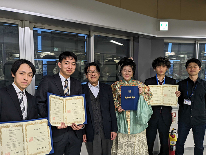
Photo with graduates of Yamada Laboratory. Third from the left is Professor Akira Yamada, far right is Assistant Professor Takahito Nishimura, and second from the right is Yosuke Abe.
What is the content of your research and how do you expect it to benefit the world?
Renewable energies are being introduced to reduce greenhouse gas emissions, and photovoltaic power generation is expected to become a key power source.
In our laboratory, we are conducting research on Cu(In,Ga)Se2 (CIGS) solar cells, which require only about 1/100th of the thickness compared to the mainstream Si solar cells. CIGSe solar cells, known for their top-tier conversion efficiency in thin-film technology, are anticipated as the next-generation solar cells due to their low cost and superior long-term reliability. Moreover, by varying the composition ratio of In and Ga, it is possible to continuously control the bandgap of CIGSe. Currently, high efficiency is obtained under In-rich conditions with a band gap of about 1.1 eV, but there is a problem that the efficiency deteriorates when the band gap is 1.4 eV, which is the theoretical limit efficiency of solar cells. To address this issue, research has been conducted on adding Ag to the CIGSe layer. The addition of Ag leads to an increase in grain size, a decrease in defect density, and enables control of the conduction and valence bands while achieving a wider bandgap. Taking advantage of these benefits, this study systematically evaluated the effects of Ag addition to CIGSe on CIGSe bulk and interface properties. As a result, it was confirmed that the open-circuit voltage of the solar cell increased by 20 mV due to the increase in the band gap near the CIGSe surface and the improvement in film quality caused by the Ag addition.
Furthermore, the back contact characteristics of CIGSe solar cells have not received much attention so far, and the carrier transport mechanisms have not been thoroughly analyzed. In this regard, we constructed a device model for CIGSe solar cells based on experimental data and conducted simulations to analyze them. As a result, it was demonstrated that a very thin MoSe2 layer of about 5 nm, which is naturally formed at the interface between CIGSe and the back electrode Mo plays a crucial role in the carrier transport of CIGSe solar cells. Moreover, by advancing the simulations, it was revealed that inserting a layer with a high acceptor density at the Mo/CIGSe interface improves the back contact characteristics. This finding provides guideline for further enhancing the efficiency of CIGSe solar cells.
Comments on the award
I am very honored to receive the Outstanding Master Student Award. I would like to thank all the professors and laboratory members who guided me in my research and helped me to achieve this result. I would like to take this opportunity to thank everyone who has helped me.
I will continue my doctoral course from next year onward, and I will focus even more on my research, aiming to contribute to the realization of a sustainable society.
