Electrical and Electronic Engineering News
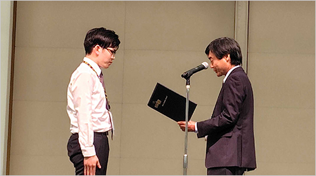
Selected as a "Highlighted Presentation" at the 70th JSAP Spring Meeting
Successful spatially-resolved measurement of electron temperature and density - Joint research by Tokyo Tech and ULVAC
In the manufacturing process of semiconductor integrated circuits, complicated pattern formation such as deep etching is performed by irradiation of reactive plasma. Such microfabrication technology is called "plasma etching", and it has become an indispensable technology for the fabrication of large-scale integrated circuits. However, at present, equipment control during plasma etching is usually performed by adjusting the operating parameters of the equipment, such as the flow rate, composition, and pressure of the raw material gas for generating plasma, and plasma discharge power. It relies heavily on experience. Ideally, the physical quantities that characterize the "plasma" used in microfabrication, such as "electron temperature and density," should be accurately measured at each location in the equipment to ensure the quality and yield of the semiconductor devices being processed. Although it is indispensable for improvement, the non-equilibrium characteristics of "plasma" have made it difficult to interpret them even if simple optical emission spectroscopic measurement is performed.
As a solution to this, at the Tokyo Institute of Technology "ULVAC Advanced Technology Collaborative Research Cluster", Mr. Yuya Yamashita, a first-year doctoral student in the electrical and electronic course, is playing a central role in applying the non-equilibrium plasma measurement method cultivated over many years in the Akatsuka laboratory to semiconductor technology. They succeeded in obtaining the electron temperature and density by applying it to the plasma of the process equipment, including tomographic measurement. In order to announce this result, they applied for a presentation at the 70th Japan Society of Applied Physics Spring Meeting. At the Akatsuka Laboratory, they have modeled the chemical network of excitation kinetics in plasma based on elementary processes, and have shown the feasibility of optical emission spectroscopic measurements to determine electron temperature and density. Through the past year and a half of joint research at the ULVAC Advanced Technology Collaborative Research Cluster, by applying the research results to a plasma irradiation device simulating an actual machine, space-resolved measurement of the electron temperature and density of semiconductor process plasma has been achieved.
For details, see the website of the Japan Society of Applied Physics![]() .
.
Every meeting, there are about 4,000 presentations, and about 20 of them are chosen as the highlighted presentation.
Also, Tokyo Tech "ULVAC Advanced Technology Collaborative Research Cluster"![]() was launched in September 2021 thanks to the efforts of Tokyo Tech. "Open Innovation Platform".
was launched in September 2021 thanks to the efforts of Tokyo Tech. "Open Innovation Platform".
Since then, they have been conducting joint research with the aim of improving the performance of plasma processing equipment. As mentioned above, the joint research for a year and a half has produced results that have been designated as highlighted presentation at JSAP meeting. Tokyo Tech and Ulvac are aiming for further sophistication and social implementation, and will make further efforts. Please stay tuned.
- The 70th Japan Society of Applied Physics Spring Academic Lecture "Featured Lecture" - Spatial-resolved optical emission spectroscopic measurement of electron temperature and density in semiconductor process plasma(in Japanese)
- Akatsuka laboratory
- Yuya Yamashita (D1) of Akatsuka Lab won the GEC Student-Poster Prize at the 75th Annual Gaseous Electronics Conference|Electrical and Electronic Engineering News
- ULVAC, Inc.
Contact
Associate Professor Hiroshi Akatsuka
Institute of Innovative Research,
Tokyo Institute of Technology
E-mail : hakatsuk@lane.iir.titech.ac.jp
※March 13, 14:30 Some links in this article have been changed.
Featured News
![]()