Electrical and Electronic Engineering News
A Novel 640 Gbps Chipset Paves the Way for Next Generation Wireless Systems
The chipset, consisting of transmitter and receiver integrated circuits, operates in D-band and offers speeds 10 to 100 times faster than 5G systems.
A new D-band CMOS transceiver chipset with 56 GHz signal-chain bandwidth achieves the highest transmission speed of 640 Gbps for a wireless device realized with integrated circuits, as reported by researchers from Tokyo Tech and National Institute of Information and Communications Technology. The proposed chipset is highly promising for the next generation of wireless systems.
To achieve faster speeds and handle increasing data traffic, wireless systems are operating in higher millimeter-wave frequency bands. Current high-band 5G systems offer speeds as high as 10 Gbps and operate in frequency bands between 24–47 GHz. The next generation of mobile communication systems, is exploring even higher frequency bands.
Within this spectrum, the D-band, covering frequencies from 110 to 170 GHz, is expected to play a crucial role in the development of next generation of wireless systems. While high frequencies provide faster data speeds, they are susceptible to attenuation. Therefore, for the widespread adoption of next generation of wireless systems, cost-effective transmitters and receivers capable of maintaining signal strength are crucial.
Recently, Professor Kenichi Okada and his team at Tokyo Institute of Technology, in collaboration with National Institute of Information and Communications Technology (NICT), Japan, have developed a novel transceiver chipset for the D-band. This chipset is fabricated using the widely-used 65nm silicon Complementary Metal-Oxide-Semiconductor (CMOS) process, making it cost-effective for mass production. The research results were presented at the 2024 IEEE Symposium on VLSI Technology & Circuits, June 16–20 in Honolulu, USA.![]()
Okada remarks, "Notably, the world's highest wireless transmission rate of 640 Gbps is achieved using low-cost CMOS technology."
This work presents a D-band (114–170 GHz) CMOS transceiver chipset covering a 56 GHz signal-chain bandwidth. The transceiver, with a chip size of 1.87 mm x 3.30 mm for the transmitter integrated circuit (IC) and 1.65 mm x 2.60 mm for the receiver IC, uses components designed to maintain signal speed and quality across a broad frequency spectrum (refer to Figure 1). These include power amplifiers for elevating signals to suitable levels, low-noise amplifiers for boosting signal strength while minimizing noise, frequency converters (mixers) for adjusting signals to the desired frequency range, distributed amplifiers for linearity, and frequency multipliers for quadrupling the frequency.
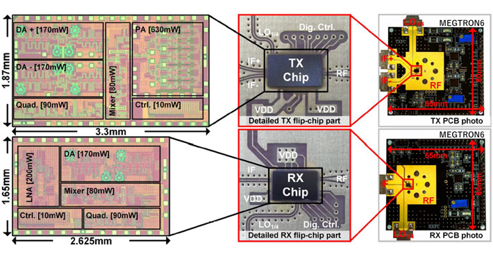
Figure 1. Transceiver chipset micrograph and PCB photo
- The fabricated D-band transmitter/receiver chipset: (Top) Transmitter, (Bottom) Receiver, (Left) CMOS transmitter/receiver IC, (Middle) Flip-chip mounted IC chip, and (Right) Entire board.
To assess the wireless transmission capabilities, the researchers mounted the chipset on a PCB and connected it to an external antenna with a gain of 25 dBi. The signal was converted from a transmission line format, typically used on PCBs, to a waveguide format, used for high-frequency signal transmission in wireless applications, with the conversion loss kept to 4 dB. With the new chipset, the researchers achieved high linearity for multi-level modulation schemes like 16QAM and 32QAM (QAM: Quadrature Amplitude Modulation), solving a major roadblock for IC transceivers (check Figure 2).
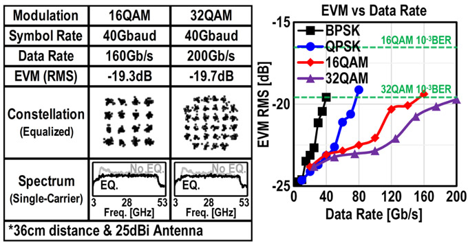
Figure 2. Results of wireless transmission measurement at a short distance (36 cm)
- Single-input single-output over-the-air measurement with 25 dBi antenna.
- Single-input single-output over-the-air measurement with 25 dBi antenna.
In testing with a modulated signal with a symbol rate of 40 Gbaud and 32QAM modulation at a distance of 36 cm, the system achieved a transmission speed of 200 Gbps with high modulation accuracy, with a bit error rate of less than 10-3. Furthermore, using 16QAM modulation and a high-gain antenna (with a gain of 43 dBi), the researchers were able to achieve speeds of 120 Gbps over a distance of 15 m (as shown in Figure 3).
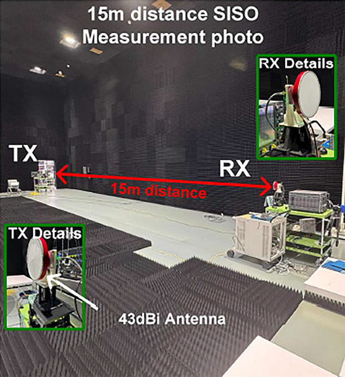
Figure 3. Wireless transmission measurement
- A photo depicting the single-input single-output measurement at a transmission distance of 15m in B5G anechoic chamber building of NICT.
The chipset's performance was further impressive in a multiple-input multiple-output configuration with four transmitters and four receiver modules. Here, each antenna can handle its own data stream, enabling fast communication. Using 16QAM modulation, each channel reached a speed of 160 Gbps. Overall, this resulted in a total speed of 640 Gbps.
These speeds represent a significant leap, being 10 to 100 times faster than current 5G systems. Okada concludes: "The proposed chipset holds promise for the next generation of wireless systems to support automated cars, telemedicine, and advanced virtual reality experiences."
This work is partially supported by the Ministry of Internal Affairs and Communications in Japan (JPJ000254).
- Reference
| Conference : | The 2024 IEEE Symposium on VLSI Technology & Circuits |
| Session : | C9 Wireless Transceivers (June 18, 3:50PM, Honolulu, USA, local time) |
| Session title : | A 640-Gb/s 4×4-MIMO D-Band CMOS Transceiver Chipset |
| Authors : | Chenxin Liu1, Zheng Li1, Yudai Yamazaki1, Hans Herdian1, Chun Wang1, Anyi Tian1, Jun Sakamaki1, Han Nie1, Xi Fu1, Sena Kato1, Wenqian Wang1, Hongye Huang1, Shinsuke Hara2, Akifumi Kasamatsu2, Hiroyuki Sakai1, Kazuaki Kunihiro1, Atsushi Shirane1, and Kenichi Okada1* |
| Affiliations : |
1 Tokyo Institute of Technology, Japan 2 National Institute of Information and Communications Technology, Japan |
|
* Corresponding author's email: okada@ee.e.titech.ac.jp (Kenichi Okada) |
|
- Combating Fractional Spurs in Phase Locked Loops to Improve Wireless System Performance in Beyond 5G | Tokyo Tech News
- Tapping into the 300 GHz Band with an Innovative CMOS Transmitter | Tokyo Tech News
- World's First Successful High-Speed Data Transmission with Beamforming in 300 GHz Band | Tokyo Tech News
- Towards the New-Space Era with Foldable Phased-Array Transmitters for Small Satellites | Tokyo Tech News
- Preparing the Stage for 6G: A Fast and Compact Transceiver for Sub-THz Frequencies | Tokyo Tech News
- Improving the Performance of Satellites in Low Earth Orbit | Tokyo Tech News
- New Transmitter Design for Small Satellite Constellations Improves Signal Transmission | Tokyo Tech News
- Novel Architecture Can Reduce Noise-Induced Jitters in Digital Technology | Tokyo Tech News
- New and Improved Multi-Band Operational Receiver for 5G New Radio Communication | Tokyo Tech News
- Efficient Satellite Downlink with a Ka Band Dual Circular Polarization Transmitter | Tokyo Tech News
- Electricity and Data Over-the-Air: The Simultaneous Transmission of 5G and Power | Tokyo Tech News
- Introducing a Transceiver that Can Tap into the Higher Frequency Bands of 5G Networks | Tokyo Tech News
- Novel Fast-Beam-Switching Transceiver Takes 5G to the Next Level | Tokyo Tech News
- Lean and mean: Maximizing 5G communications with an energy-efficient relay network | Tokyo Tech News
- Pushed to the Limit: A CMOS-based transceiver for beyond 5G applications at 300 GHz | Tokyo Tech News
- Greater Connectedness in Remote Areas: A Ka-band Transceiver for Satellite Communications | Tokyo Tech News
- Researchers develop a compact 28-GHz transceiver supporting dual-polarized MIMO | Tokyo Tech News
- Three Tokyo Tech Faculty Members to Receive 2023 IEEE Fellow Titles | Tokyo Tech News
- Kenichi Okada - Wiring the world wirelessly | Research Stories | Research
- Kenichi Okada | Researcher Finder - Tokyo Tech STAR Search
- Okada Laboratory
- Electrical and Electronic Engineering Graduate Major|Education|Department of Electrical and Electronic Engineering, School of Engineering
- Electrical and Electronic Engineering Undergraduate Major|Education|Department of Electrical and Electronic Engineering, School of Engineering
- National Institute of Information and Communications Technology (NICT)
- Latest Research News

School of Engineering
—Creating New Industries and Advancing Civilization—
Information on School of Engineering inaugurated in April 2016
Further Information
Professor Kenichi Okada
School of Engineering, Tokyo Institute of Technology
Email okada@ee.e.titech.ac.jp
Tel +81-3-5734-3764
Featured News


![]()