Electrical and Electronic Engineering News
Combating Fractional Spurs in Phase Locked Loops to Improve Wireless System Performance in Beyond 5G
Two innovative design techniques lead to substantial improvements in performance in fractional-N phase locked loops (PLLs), report scientists from Tokyo Tech. The proposed methods are aimed to minimize unwanted signals known as fractional spurs, which typically plague PLLs used in many modern radar systems and wireless transceivers. These efforts could open doors to technological improvements in wireless communication, autonomous vehicles, surveillance, and tracking systems in beyond 5G era.
Many emerging and evolving technologies, such as self-driving vehicles, target tracking systems, and remote sensors, rely on the high-speed and error-free operation of wireless data transceivers and radar systems. In these applications, phase locked loops (PLLs) are crucial components that help with the synthesis, modulation, and synchronization of oscillating signals. Thus, eliminating or minimizing sources of error in PLLs is essential to improve the overall performance of systems.
In fractional-N PLLs, a popular type of PLL with excellent resolution and flexible control of frequency, jitter and fractional spurs are mainstay enemies. "Jitter" refers to the overall deviation from the ideal timing of the synthesized oscillation. On the other hand, fractional spurs are unwanted signals that arise from the periodicity in the error. Components called digital-to-time converters (DTCs) are typically used in the digital PLLs to cancel the quantization error, but imperfections in DTCs due to so-called "integral non-linearities (INLs)" ultimately manifest as fractional spurs that degrade phase noise in the output of the PLL.
In a recent study, a research team from Tokyo Institute of Technology (Tokyo Tech), led by Professor Kenichi Okada, sought to address these problems through the development of two innovative design techniques leading to a low-spur fractional-N PLL. Their work has been published in the Proceeding of the 2024 IEEE International Solid-State Circuits Conference (ISSCC)![]() .
.
The first proposed technique involves the use of a cascaded-fractional divider. This method involves splitting the frequency control word (FCW), an internal PLL signal that controls the output frequency, into two but in a way that both are far from an integer value. The logic underlying this is that for far-integer FCWs, fractional spurs appear in the PLL in higher frequencies, and high-frequency components are naturally filtered out by the inherent operations of the PLL (Figure 1). Notably, this approach does not involve digital pre-distortion (DPD), a technique that introduces complexity and causes slower phase locking.
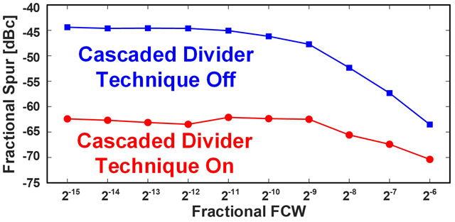
Figure 1. Supression of fractional spurs.
- The proposed cascaded divider technique achieves a substantially improved PLL performance by minimizing fractional spurs.
The second proposed technique revolves around a pseudo-differential DTC to avoid the pitfalls of standard DTC implementations (Figure 2). "In conventional DTC designs, there are stringent trade-offs between the DTC power, delay range, noise, and INL, limiting the minimum fractional-spur level achievable," explains Prof. Okada. To tackle this issue, the researchers noted that the non-linearities of DTCs contain even symmetric components. Accordingly, they implemented the function of a single DTC using two half-range DTCs with the same even-symmetric INLs in differential operation. As a result, these INLs were naturally cancelled out via subtraction at the PLL's phase detector.
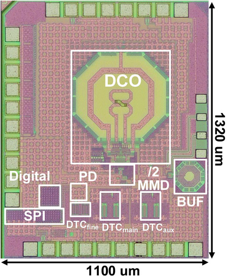
Figure 2. Die micrograph of the proposed digital phase locked loop (PLL).
- The total power consumption of the proposed PLL is only 8.89 mW from a 1 V supply, which leads to a figure of merit of reference of -247.4 dB.
The team tested their ideas by implementing the proposed digital PLL using a 65 nm CMOS process, requiring an active circuit area of only 0.23 mm2. By comparing the performance of their device with other state-of-the-art designs, the researchers noted several advantages. "By suppressing fractional spurs, the integrated PLL jitter was reduced from 243.5 fs to 143.7 fs," highlights Prof. Okada. "Thanks to the proposed cascaded fractional divider and pseudo-differential DTC techniques, we achieved the lowest class of jitter without DPD technology."
With any luck, this innovative design will lead to technological improvements across many applications where fractional-N PLLs are a mainstay.
These research results were partially obtained from the commissioned research (No. JPJ012368C00801) by National Institute of Information and Communications Technology (NICT), Japan.
- Reference
| Conference : |
2024 IEEE International Solid-State Circuits Conference (ISSCC) |
| Session : | Session 10 – Frequency Synthesis (February 20, 8:50AM, PST) |
| Session Title : | A 7GHz Digital PLL with Cascaded Fractional Divider and Pseudo-Differential DTC Achieving -62.1dBc Fractional Spur and 143.7fs Integrated Jitter |
| Journal : | Proceeding of the 2024 IEEE International Solid-State Circuits Conference (ISSCC) |
| Authors : | Dingxin Xu1, Zezheng Liu1, Yifeng Kuai1, Hongye Huang1, Yuncheng Zhang1, Zheng Sun1, Bangan Liu1, Wenqian Wang1, Yuang Xiong1, Junjun Qiu1, Waleed Madany1, Yi Zhang1, Ashbir Aviat Fadila1, Atsushi Shirane1, and Kenichi Okada1 |
| Affiliations : | 1Tokyo Institute of Technology, Japan |
- Tapping into the 300 GHz Band with an Innovative CMOS Transmitter | Tokyo Tech News
- World's First Successful High-Speed Data Transmission with Beamforming in 300 GHz Band | Tokyo Tech News
- Towards the New-Space Era with Foldable Phased-Array Transmitters for Small Satellites | Tokyo Tech News
- Preparing the Stage for 6G: A Fast and Compact Transceiver for Sub-THz Frequencies | Tokyo Tech News
- New Transmitter Design for Small Satellite Constellations Improves Signal Transmission | Tokyo Tech News
- Novel Architecture Can Reduce Noise-Induced Jitters in Digital Technology | Tokyo Tech News
- Improving the Performance of Satellites in Low Earth Orbit | Tokyo Tech News
- New and Improved Multi-Band Operational Receiver for 5G New Radio Communication | Tokyo Tech News
- Efficient Satellite Downlink with a Ka Band Dual Circular Polarization Transmitter | Tokyo Tech News
- Introducing a Transceiver that Can Tap into the Higher Frequency Bands of 5G Networks
- Electricity and Data Over-the-Air: The Simultaneous Transmission of 5G and Power | Tokyo Tech News
- Novel Fast-Beam-Switching Transceiver Takes 5G to the Next Level | Tokyo Tech News
- Lean and mean: Maximizing 5G communications with an energy-efficient relay network | Tokyo Tech News
- Pushed to the Limit: A CMOS-based transceiver for beyond 5G applications at 300 GHz | Tokyo Tech News
- Greater Connectedness in Remote Areas: A Ka-band Transceiver for Satellite Communications | Tokyo Tech News
- Researchers develop a compact 28-GHz transceiver supporting dual-polarized MIMO | Tokyo Tech News
- Smallest all-digital circuit opens doors to 5 nm next-gen semiconductor | Tokyo Tech News
- Three Tokyo Tech Faculty Members to Receive 2023 IEEE Fellow Titles | Tokyo Tech News
- Kenichi Okada - Wiring the world wirelessly | Research Stories | Research
- Kenichi Okada | Researcher Finder - Tokyo Tech STAR Search
- Okada Laboratory
- Electrical and Electronic Engineering Graduate Major|Education|Department of Electrical and Electronic Engineering, School of Engineering
- Electrical and Electronic Engineering Undergraduate Major|Education|Department of Electrical and Electronic Engineering, School of Engineering
- Latest Research News
School of Engineering
—Creating New Industries and Advancing Civilization—
Information on School of Engineering inaugurated in April 2016
Further Information
Professor Kenichi Okada
School of Engineering, Tokyo Institute of Technology
Email okada@ee.e.titech.ac.jp
Tel +81-3-5734-3764

