Electrical and Electronic Engineering News
How Flawed Diamonds ”Lead” to Flawless Quantum Networks
Lead-based vacancy centers in diamonds that form after high-pressure and high-temperature treatment are ideal for quantum networks, find Tokyo Institute of Technology (Tokyo Tech) scientists. The modified crystal system could also find applications in spintronics and quantum sensors.
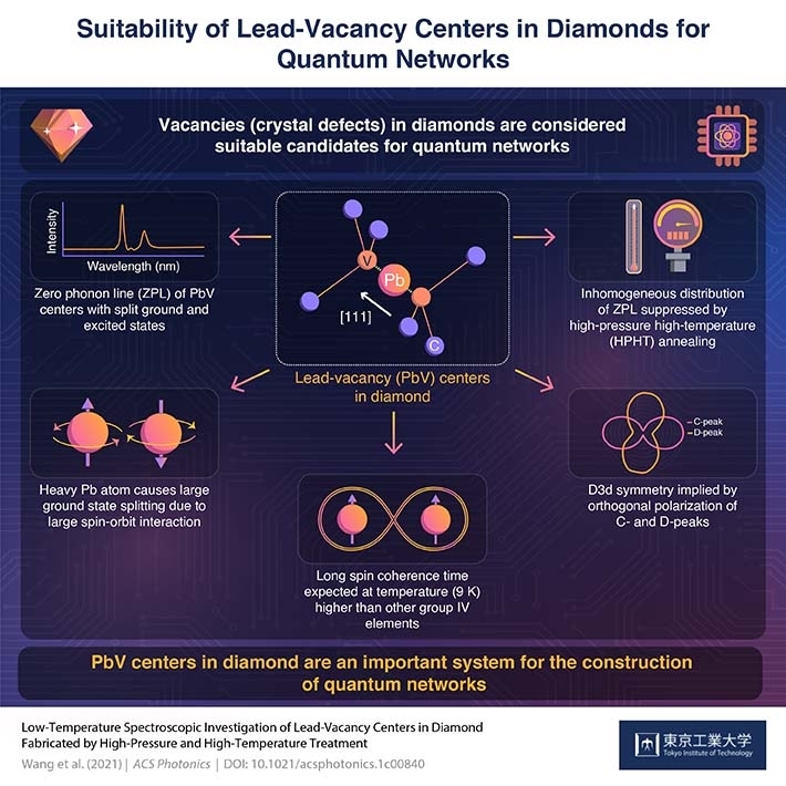
The color in a diamond comes from a defect, or "vacancy," where there is a missing carbon atom in the crystal lattice. Vacancies have long been of interest to electronics researchers because they can be used as ‘quantum nodes' or points that make up a quantum network for the transfer of data. One of the ways of introducing a defect into a diamond is by implanting it with other elements, like nitrogen, silicon, or tin. In a recent study published in ACS Photonics![]() , scientists from Japan demonstrate that lead-vacancy centers in diamond have the right properties to function as quantum nodes. "The use of a heavy group IV atom like lead is a simple strategy to realize superior spin properties at increased temperatures, but previous studies have not been consistent in determining the optical properties of lead-vacancy centers accurately," says Associate Professor Takayuki Iwasaki of Tokyo Institute of Technology (Tokyo Tech), who led the study.
, scientists from Japan demonstrate that lead-vacancy centers in diamond have the right properties to function as quantum nodes. "The use of a heavy group IV atom like lead is a simple strategy to realize superior spin properties at increased temperatures, but previous studies have not been consistent in determining the optical properties of lead-vacancy centers accurately," says Associate Professor Takayuki Iwasaki of Tokyo Institute of Technology (Tokyo Tech), who led the study.
The three critical properties researchers look for in a potential quantum node are symmetry, spin coherence time, and zero phonon lines (ZPLs), or electronic transition lines that do not affect "phonons," the quanta of crystal lattice vibrations. Symmetry provides insight into how to control spin (rotational velocity of subatomic particles like electrons), coherence refers to an identicalness in the wave nature of two particles, and ZPLs describe the optical quality of the crystal.
The researchers fabricated the lead-vacancies in diamond and then subjected the crystal to high pressure and high temperature. They then studied the lead vacancies using photoluminescence spectroscopy, a technique that allows you to read the optical properties and to estimate the spin properties. They found that the lead-vacancies had a type of dihedral symmetry, which is appropriate for the construction of quantum networks. They also found that the system showed a large "ground state splitting," a property that contributes to the coherence of the system. Finally, they saw that the high-pressure high-temperature treatment they inflicted upon the crystals suppressed inhomogeneous distribution of ZPLs by recovering the damage done to the crystal lattice during the implantation process. A simple calculation showed that lead-vacancies had a long spin coherence time at a higher temperature (9K) than previous systems with silicon and tin vacancies.
"The simulation we presented in our study seems to suggest that the lead-vacancy center will likely be an essential system for creating a quantum light-matter interface—one of the key elements in the application of quantum networks," concludes an optimistic Dr. Iwasaki.
This study paves the way for the future development of large (defective) diamond wafers and thin (defective) diamond films with reliable properties for quantum network applications.
- Reference
| Authors : | Peng Wang1, Takashi Taniguchi2, Yoshiyuki Miyamoto3, Mutsuko Hatano1, and Takayuki Iwasaki1,* |
|---|---|
| Title of original paper : | Low-Temperature Spectroscopic Investigation of Lead-Vacancy Centers in Diamond Fabricated by High-Pressure and High-Temperature Treatment |
| Journal : | ACS Photonics |
| DOI : | 10.1021/acsphotonics.1c00840 |
| Affiliations : |
1 Department of Electrical and Electronic Engineering, School of Engineering, Tokyo Institute of Technology, Japan 2 International Center for Materials Nanoarchitectonics, National Institute for Materials Science, Japan 3 Research Center for Computational Design of Advanced Functional Materials, National Institute of Advanced Industrial Science and Technology, Japan |
* Corresponding author's email: iwasaki.t.aj@m.titech.ac.jp
- Artificially introduced atomic-level sensors enable measurements of the electric field within a working semiconductor device | Tokyo Tech News
- New diamond structures produce bright luminescence for quantum cryotography and biomarkers applications | Tokyo Tech News
- Quantum science and technology | Research Stories | Research
- Mutsuko Hatano - Diamonds as the ultimate semiconductors | Research Stories | Research
- Six Tokyo Tech faculty members receive FY2019 MEXT Commendation | Tokyo Tech News
- Hatano & Iwasaki Lab.
- Researcher Profile | Tokyo Tech STAR Search - Takayuki Iwasaki
- Researcher Profile | Tokyo Tech STAR Search - Mutsuko Hatano
- Electrical and Electronic Engineering Graduate Major|Education|Department of Electrical and Electronic Engineering, School of Engineering
- Energy Science and Engineering Graduate Major|Education|Department of Electrical and Electronic Engineering, School of Engineering
- National Institute for Materials Science
- National Institute of Advanced Industrial Science and Technology
- Latest Research News

School of Engineering
—Creating New Industries and Advancing Civilization—
Information on School of Engineering inaugurated in April 2016
Further Information
Associate Professor Takayuki Iwasaki
School of Engineering, Tokyo Institute of Technology
Featured News


![]()