Electrical and Electronic Engineering News
Smallest all-digital circuit opens doors to 5 nm next-gen semiconductor
Scientists at Tokyo Institute of Technology (Tokyo Tech) and Socionext Inc. have designed the world's smallest all-digital phase-locked loop (PLL). PLLs are critical clocking circuits in virtually all digital applications, and reducing their size and improving their performance is a necessary step to enabling the development of next-generation technologies.
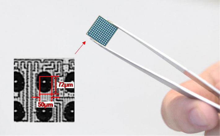
Figure 1. Photograph of a chip containing the proposed PLL
The entire all-digital PLL fits in a 50 × 72 µm2 region, making it the smallest PLL to date.
New or improved technologies, such as artificial intelligence, 5G cellular communications, and the Internet-of-Things, are expected to bring revolutionary changes in society. But for that to happen, high-performance system-on-a-chip (SoC)—a type of integrated circuit—devices are indispensable. A core building block of SoC devices is the phase-locked loop (PLL), a circuit that synchronizes with the frequency of a reference oscillation and outputs a signal with the same or higher frequency. PLLs generate ‘clocking signals’, whose oscillations act as a metronome that provides a precise timing reference for the harmonious operation of digital devices.
For high performance SoC devices to be realized, fabrication processes for semiconductor electronics must become more sophisticated. The smaller the area to implement digital circuitry is, the better the performance of the device. Manufacturers have been racing to develop increasingly smaller semiconductors. 7 nm semiconductors (a massive improvement over their 10 nm predecessor) are already in production, and methods to build 5 nm ones are now being looked at.
However, in this endeavor stands a major bottleneck. Existing PLLs require analog components, which are generally bulky and have designs that are difficult to scale down.
Scientists at Tokyo Tech and Socionext Inc., led by Prof. Kenichi Okada, have addressed this issue by implementing a 'synthesizable' fractional-N PLL, which only requires digital logic gates, and no bulky analog components, making it easy to adopt in conventional miniaturized integrated circuits.
Okada and team used several techniques to decrease the required area, power consumption and jitter—unwanted time fluctuations when transmitting digital signals—of their synthesizable PLLs. To decrease area, they employed a ring oscillator, a compact oscillator that can be easily scaled down. To suppress jitter, they reduced the phase noise—random fluctuations in a signal—of this ring oscillator, using 'injection locking'—the process of synchronizing an oscillator with an external signal whose frequency (or multiple of it) is close to that of the oscillator—over a wide range of frequencies. The lower phase noise, in turn, reduced power consumption.
The design of this synthesizable PLL beats that of all other current state-of-the-art PLLs in many important aspects. It achieves the best jitter performance with the lowest power consumption and smallest area (as can be seen in Figure 1). “The core area is 0.0036 mm2, and the whole PLL is implemented as one layout with a single power supply,” remarks Okada. Further, it can be built using standard digital design tools, allowing for its rapid, low-effort, and low-cost production, making it commercially viable.
This synthesizable PLL can be easily integrated into the design of all-digital SoCs, and is commercially viable, making it valuable for developing the much sought after 5 nm semiconductor for cutting-edge applications including artificial intelligence, internet of things and many others, where high performance and low power consumption would be the critical requirements. But the contributions of this research go beyond these possibilities. “Our work demonstrates the potential of synthesizable circuits. With the design methodology employed here, other building blocks of SoCs, such as data converters, power management circuits, and wireless transceivers, could be made synthesizable as well. This would greatly boost design productivity and considerably reduce design efforts,” explains Okada. Tokyo Tech and Socionext will continue their collaboration in this filed to advance the miniaturization of electronic devices, enabling the realization of newer-generation technologies.
This research work was conducted in cooperation with TeraPixel Technologies Inc.
Table I Performance comparison of PLLs in sub-20 nm CMOS processes
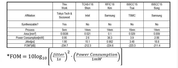
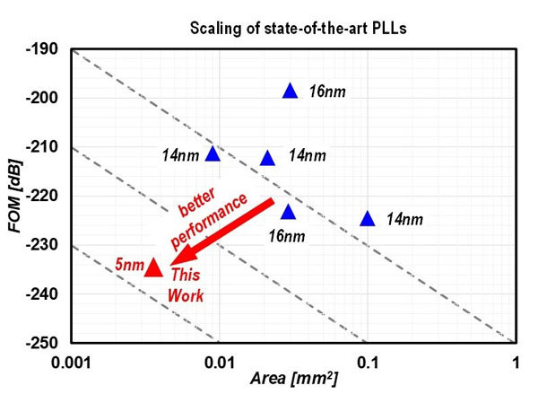
Figure 2. FOM and area comparison of PLLs in sub-20 nm CMOS processes
- Reference
| Authors : | Bangan Liu1, Yuncheng Zhang1, Junjun Qiu1, Hongye Huang1, Zheng Sun1, Dingxin Xu1, Haosheng Zhang1, Yun Wang1, Jian Pang1, Zheng Li1, Xi Fu1, Atsushi Shirane1, Hitoshi Kurosu2, Yoshinori Nakane2, Shunichiro Masaki2, Kenichi Okada1 |
|---|---|
| Title of original paper : | A Fully-Synthesizable Fractional-N Injection-Locked PLL for Digital Clocking with Triangle/Sawtooth Spread-Spectrum Modulation Capability in 5 nm CMOS |
| Journal : | IEEE Solid-State Circuits Letters |
| DOI : | 10.1109/LSSC.2020.2967744 |
| Affiliations : |
1 Tokyo Institute of Technology, Tokyo, Japan 2 Socionext Inc., Yokohama, Japan |
- A more accurate, low-cost 39 GHz beamforming transceiver for 5G communications | Tokyo Tech News
- Gearing up for 5G: A miniature, low-cost transceiver for fast, reliable communications | Tokyo Tech News
- Tinier and less power-hungry quantum atomic clock push toward intelligent IoT | Tokyo Tech News
- An ultra-low-power frequency synthesizer targeted for IoT devices: Digital PLL achieves a power consumption of 0.265 mW | Tokyo Tech News
- Tokyo Tech slashes power consumption in Bluetooth Low-Energy transceiver by more than half | Tokyo Tech News
- New 28-GHz transceiver paves the way for future 5G devices | Tokyo Tech News
- Ultra high-speed IC capable of wireless transmission of 100 gigabits per second in a 300 GHz band | Tokyo Tech News
- Speeding up adoption of 5G! Wireless transmission speeds of 120 Gbps achieved | Tokyo Tech News
- 28Gb/s wireless data rate achieved with millimeter-wave transceiver | Tokyo Tech News
- Kenichi Okada - Wiring the world wirelessly | Research Stories | Research
- Matsuzawa and Okada Laboratory won NE Analog Innovation Award | Electrical and Electronic Engineering News
- Okada Lab.
- Researcher Profile | Tokyo Tech STAR Search - Kenichi Okada
- Socionext Inc.
- TeraPixel Technologies Inc
- Latest Research News

School of Engineering
—Creating New Industries and Advancing Civilization—
Information on School of Engineering inaugurated in April 2016
Further Information
Professor Kenichi Okada
School of Engineering, Tokyo Institute of Technology
Email: okada@ee.e.titech.ac.jp
Tel +81-3-5734 -3764
Featured News

![]()