Electrical and Electronic Engineering News
Tokyo Tech slashes power consumption in Bluetooth Low-Energy transceiver by more than half
Eyeing future of IoT
Researchers at Tokyo Institute of Technology (Tokyo Tech) announce a Bluetooth Low-Energy transceiver with the lowest ever power consumption — a breakthrough set to accelerate widespread adoption of Internet of Things (IoT) applications in Japan and around the globe.
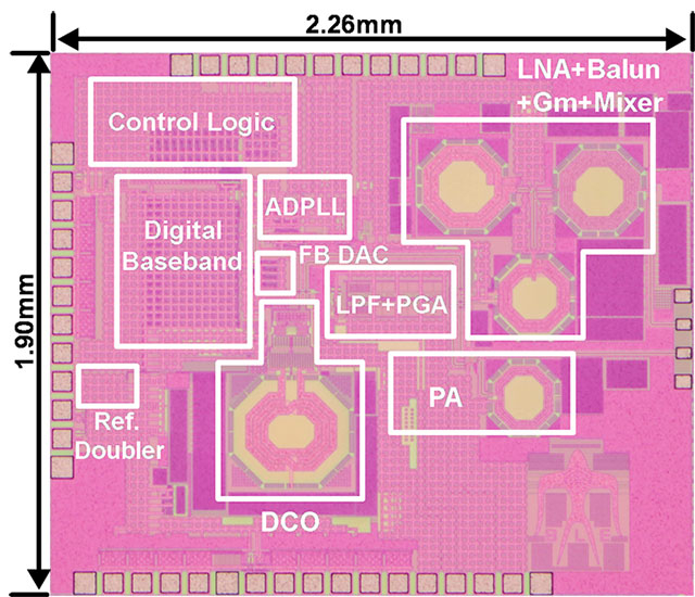
Figure. A photograph of the chip
The chip was designed using standard 65-nanometer CMOS technology.
An ultra-low-power Bluetooth Low-Energy transceiver designed for use in the popular 2.4 GHz band has been developed by a group of researchers led by Kenichi Okada of Tokyo Institute of Technology, Japan.
When transmitting, the transceiver consumes 2.9 milliwatts (mW) and when receiving, it consumes just 2.3 mW. Given that minimizing power consumption is a requirement for the oncoming IoT era, these figures are remarkable, as they represent less than half the power consumed by previous transceivers (see Table).
Table. A performance comparison of BLE transceivers
Tokyo Tech's BLE transceiver achieves a dramatic reduction in power consumption — down to less than half of those previously reported. All figures are in milliwatts (mW).
| Transmitter | Receiver | |
| Tokyo Tech ISSCC 2018 | 2.9 | 2.3 |
| Renesas ISSCC 2015 | 7.7 | 6.3 |
| Dialog ISSCC 2015 | 10.1 | 11.2 |
| Texas Instruments CC2540 | 63 | 58 |
| Nordic nRF51822 | 32 | 32 |
Why BLE matters
Within the next decade, IoT is projected to become a multi-trillion US dollar industry. Bluetooth Low-Energy (BLE) is in the spotlight as a key technology spurring the growth of this fast-evolving market. Already embedded in millions of Apple and Android devices, BLE is the most used short-range wireless technology aimed at low-power and low-cost connectivity.
Low-energy solutions are in demand not only for smartphones and watches, but also for emerging applications in the medical and healthcare fields, factories and public infrastructure such as roads, bridges and tunnels. IoT sensors for early detection and warning systems could mean the difference between life and death.
"Our research grew out of this need for connectivity," explains Okada. "In an IoT world, trillions of devices will be used. To extend battery life and aim for maintenance-free operations, reducing power consumption is vital."
Key features
The BLE transceiver has excellent receiver sensitivity1 and high interference tolerance2, while also realizing the lowest power consumption.
The transmitter employs an all-digital phase-locked loop (ADPLL), an attractive building block for BLE, as it is less susceptible to noise compared to its analog counterpart. The transceiver was designed in a 65-nanometer CMOS process3.
In another study focusing on ADPLL, the researchers achieved a figure of merit (FoM)4 of -246 dB, one of the best obtained so far. The FoM is an important metric for evaluating the trade-off between performance and power consumption.
The above results arose from a project supported by Japan's New Energy and Industrial Technology Development Organization (NEDO).
Looking ahead
In future, Okada says: "The PLL could operate on just 0.65 mW, and studies are underway to reduce our transceiver's power consumption even further."
The team will present their findings at the 2018 International Solid-State Circuits Conference (ISSCC). Held every February in San Francisco, the conference, popularly known as the Chip Olympics, is regarded as the leading forum on integrated circuit research and development.
1 Receiver sensitivity : A measure of how well a receiver can pick up the tiniest of signals. The figure reached in this study was an impressive -94 decibels relative to 1 milliwatt (dBm).
2 High interference tolerance : Referring to the need for high tolerance to interference from other signals operating in the busy 2.4 GHz band.
3 CMOS process : A standard method of building integrated circuits using silicon-based complementary metal–oxide–semiconductor (CMOS) technology.
4 Figure of merit (FoM) : The FoM evaluates the trade-off between jitter (related to noise in wireless communication) and power consumption. Reducing jitter is desirable for improving the quality of communication, but this requires more energy, so there is a trade-off between performance and power consumption. In general, the lower the FoM, the better. The figure of -246 dB is one of the lowest ever achieved.
Reference 1
| Authors : | Hanli Liu, Dexian Tang, Zheng Sun, Wei Deng, Huy Cu Ngo, Kenichi Okada, Akira Matsuzawa |
|---|---|
| Title of original paper : | A 0.98 mW Fractional-N ADPLL Using 10b Isolated Constant-Slope DTC with FOM of -246 dB for IoT Applications in 65 nm Session 15, RF PLLs, 2018 IEEE International Solid-State Circuits Conference |
| Affiliations : | Tokyo Institute of Technology, Tokyo, Japan |
Reference 2
| Authors : | Hanli Liu, Zheng Sun, Dexian Tang, Hongye Huang, Tohru Kaneko, Wei Deng, Rui Wu, Kenichi Okada, Akira Matsuzawa |
|---|---|
| Title of original paper : | An ADPLL-Centric Bluetooth Low-Energy Transceiver with 2.3 mW Interference-Tolerant Hybrid-Loop Receiver and 2.9 mW Single-Point Polar Transmitter in 65 nm CMOS Session 28, Wireless Connectivity, 2018 IEEE International Solid-State Circuits Conference |
| Affiliations : | Tokyo Institute of Technology, Tokyo, Japan |
- Kenichi Okada – Wireing the world wirelessly | Research Stories
- Matsuzawa & Okada Lab.
- Researcher Profile Tokyo Tech STAR Search | Akira Matsuzawa
- Researcher Profile Tokyo Tech STAR Search | Kenichi Okada
- Department of Electrical and Electronic Engineering
- Latest Research News

School of Engineering
—Creating New Industries and Advancing Civilization—
Information on School of Engineering inaugurated in April 2016
Further Information
Associate Professor Kenichi Okada
School of Engineering, Tokyo Institute of Technology
Email okada@ee.e.titech.ac.jp
Tel +81-3-5734 -2258
Featured News

![]()