Electrical and Electronic Engineering News
Compact and Scalable Multiple-Input Multiple-Output Systems for Future 5G Networks
The proposed 28GHz beamformer shares radio frequency elements for the highest area efficiency among multiple-input multiple-output receivers
A 28GHz time-division multiple-input multiple-output (MIMO) receiver with eight radio frequency elements, each occupying just 0.1 mm2, has been developed by researchers at Tokyo Tech using 65nm CMOS technology. This innovative design reduces chip size for beamforming. Achieving -23.5 dB error vector magnitude in 64-quadrature amplitude modulation and data rates up to 9.6 Gbps, this receiver offers the highest area efficiency and fastest beam switching among reported MIMO receivers.
To meet the growing need for data from applications like video streaming, augmented reality, autonomous vehicles, and Internet of Things devices, 5G New Radio and future beyond 5G technologies utilize multi-beam multiple-input multiple-output to send and receive multiple streams of data simultaneously. An essential component for effective MIMO operation is beamforming. Beamforming adjusts the signals to focus them towards the transmitters or receivers. This process improves signal quality and minimizes interference. However, conventional analog beamforming MIMO receivers require separate beamformers for each data stream, making it challenging to implement in a millimeter wave MIMO system like a 28GHz MIMO transceiver where the antenna pitch (the distance between antennas) is only 5 millimeters.
To address this, researchers led by Professor Kenichi Okada from Tokyo Institute of Technology have proposed a novel technique called time-division MIMO (TD-MIMO) beamformer that can support millimeter-wave MIMO without the need for additional hardware. The study has been published in the Proceedings of the 2024 IEEE VLSI Symposium and presented at the 2024 IEEE Symposium on VLSI Technology & Circuits![]() , June 16-20 in Honolulu, USA.
, June 16-20 in Honolulu, USA.
"The major challenge with conventional millimeter-wave MIMO receivers is that their area and power consumption increase linearly with the number of MIMO streams they need to support. As a result, the chip size scales with the number of MIMO streams. Therefore, more than three MIMO streams have never been demonstrated for a 2D array," explains Okada.
In MIMO systems, each antenna connects with every other antenna via a network of radio frequency (RF) paths. The number of these paths is determined by multiplying the number of MIMO streams by the number of antennas. Therefore, increasing the number of data streams increases the RF paths needed.
In TD-MIMO operation, an analog beamformer quickly switches the beam pattern or direction of the receiver at very high speeds, allowing multiple signals to use the same RF paths. After the beamforming process, a TD-MIMO switch directs each MIMO stream to separate output ports, ensuring that the signals do not interfere with each other.
This system uses fast-switching phase shifters which can adjust the signal phase within 2.5 nanoseconds, and clock-based synchronization to control the timing of the beam switching. This approach enables the TD-MIMO receiver to support more data streams by simply increasing the clock frequency, ensuring scalable data transmission without increasing the size of the chipset.
Researchers developed a 3mm x 2mm TD-MIMO receiver using 65nm CMOS technology consisting of 8 RF elements to handle four separate 5G New Radio data streams across a 400MHz channel bandwidth using 64-quadrature amplitude modulation (QAM). The signals pass through a Wilkinson power combiner to a TD-MIMO switch, which separates them into four paths. Each RF element features a noise-cancelling amplifier and a fast phase shifter. A variable gain amplifier and a retiming circuit keep the system in sync by ensuring the switching occurs accurately (refer to Figures 1 and 2).
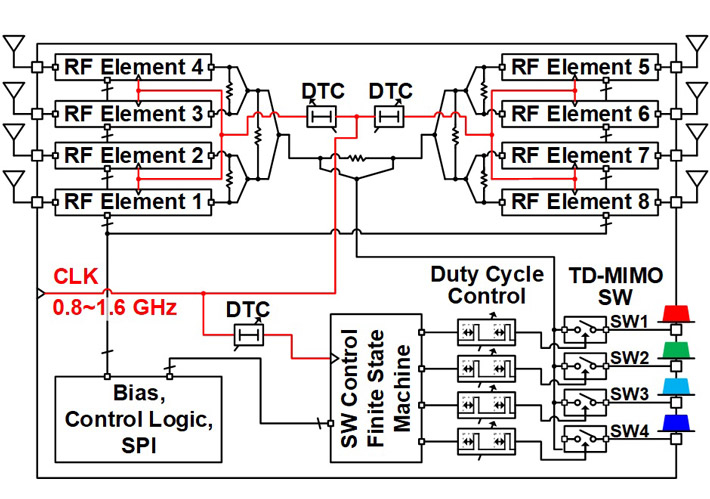
Figure 1. The block diagram of the 28 GHz beamformer designed without frequency-converting components
- A 3-stage 8-to-1 Wilkinson power combiner combines the beams, which are then separated to respective outputs by a TD-MIMO switch. An H-tree network distributes the synchronization clock to each receiver element, with DTCs in the clock distribution network for precise timing calibration.

Figure 1. The block diagram of the 28 GHz beamformer designed without frequency-converting components
A 3-stage 8-to-1 Wilkinson power combiner combines the beams, which are then separated to respective outputs by a TD-MIMO switch. An H-tree network distributes the synchronization clock to each receiver element, with DTCs in the clock distribution network for precise timing calibration.
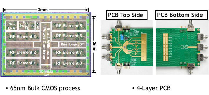
Figure 2. Chip micrograph and the photo of the printed circuit board (PCB) of the proposed TD-MIMO receiver
- The TD-MIMO receiver is fabricated using a common 65nm CMOS process making it suitable for scalable production. The PCB has four layers and integrates a 1 by 8 antenna array in the bottom layer.

Figure 2. Chip micrograph and the photo of the printed circuit board (PCB) of the proposed TD-MIMO receiver
The TD-MIMO receiver is fabricated using a common 65nm CMOS process making it suitable for scalable production. The PCB has four layers and integrates a 1 by 8 antenna array in the bottom layer.
The receiver successfully handled 5G-compliant MIMO signals from a Keysight arbitrary waveform generator transmitted by horn antennas in four directions. It achieved -23.5 dB error vector magnitude in 64-QAM and a rapid Nyquist-rate beam switching time of 0.15 ns, enabling data rates up to 9.6 Gbps across the four-stream MIMO configuration.
"This work realizes highest data rates with highest area efficiency among listed MIMO receivers," says Okada. With each RF element occupying just 0.1 mm2, the proposed chipset can pave the way to smaller and more compact efficient, scalable, multi-beam MIMO systems for high-speed data transmission.
This work is partially supported by the National Institute of Information and Communications Technology (NICT) in Japan (JPJ012368C00801).
- Reference
| Conference : | The 2024 IEEE Symposium on VLSI Technology & Circuits |
| Session : | C9 Wireless Transceivers (June 18, 5:05 PM, Honolulu, USA, local time) |
| Session title : | A 28GHz 4-Stream Time-Division MIMO Phased-Array Receiver Utilizing Nyquist-Rate Fast Beam Switching for 5G and beyond |
| Journal : | Proceedings of the 2024 IEEE VLSI Symposium |
| Authors : | Yi Zhang |
| Affiliations : |
1 Department of Electrical and Electronic Engineering, Tokyo Institute of Technology, Japan |
|---|---|
|
* Corresponding author's email: okada@ee.e.titech.ac.jp |
|
| Conference : | The 2024 IEEE Symposium on VLSI Technology & Circuits |
|---|---|
| Session : | C9 Wireless Transceivers (June 18, 5:05 PM, Honolulu, USA, local time) |
| Session title : | A 28GHz 4-Stream Time-Division MIMO Phased-Array Receiver Utilizing Nyquist-Rate Fast Beam Switching for 5G and beyond |
| Journal : | Proceedings of the 2024 IEEE VLSI Symposium |
| Authors : | Yi Zhang |
| Affiliations : |
1 Department of Electrical and Electronic Engineering, Tokyo Institute of Technology, Japan |
|
* Corresponding author's email: okada@ee.e.titech.ac.jp |
|
- Towards Wider 5G Network Coverage: Novel Wirelessly Powered Relay Transceiver | Tokyo Tech News
- Wirelessly Powered Relay Will Help Bring 5G Technology to Smart Factories | Tokyo Tech News
- A Novel 640 Gbps Chipset Paves the Way for Next Generation Wireless Systems | Tokyo Tech News
- Combating Fractional Spurs in Phase Locked Loops to Improve Wireless System Performance in Beyond 5G | Tokyo Tech News
- Tapping into the 300 GHz Band with an Innovative CMOS Transmitter | Tokyo Tech News
- World's First Successful High-Speed Data Transmission with Beamforming in 300 GHz Band | Tokyo Tech News
- Preparing the Stage for 6G: A Fast and Compact Transceiver for Sub-THz Frequencies | Tokyo Tech News
- Improving the Performance of Satellites in Low Earth Orbit | Tokyo Tech News
- New Transmitter Design for Small Satellite Constellations Improves Signal Transmission | Tokyo Tech News
- Novel Architecture Can Reduce Noise-Induced Jitters in Digital Technology | Tokyo Tech News
- New and Improved Multi-Band Operational Receiver for 5G New Radio Communication | Tokyo Tech News
- Efficient Satellite Downlink with a Ka Band Dual Circular Polarization Transmitter | Tokyo Tech News
- Electricity and Data Over-the-Air: The Simultaneous Transmission of 5G and Power | Tokyo Tech News
- Introducing a Transceiver that Can Tap into the Higher Frequency Bands of 5G Networks | Tokyo Tech News
- Novel Fast-Beam-Switching Transceiver Takes 5G to the Next Level | Tokyo Tech News
- Lean and mean: Maximizing 5G communications with an energy-efficient relay network | Tokyo Tech News
- Three Tokyo Tech Faculty Members to Receive 2023 IEEE Fellow Titles | Tokyo Tech News
- Kenichi Okada - Wiring the world wirelessly | Research Stories | Research
- Kenichi Okada | Researcher Finder - Tokyo Tech STAR Search
- Okada Laboratory
- Electrical and Electronic Engineering Graduate Major|Education|Department of Electrical and Electronic Engineering, School of Engineering
- Electrical and Electronic Engineering Undergraduate Major|Education|Department of Electrical and Electronic Engineering, School of Engineering
- Latest Research News
School of Engineering
—Creating New Industries and Advancing Civilization—
Information on School of Engineering inaugurated in April 2016
Further Information
Professor Kenichi Okada
School of Engineering,
Tokyo Institute of Technology
Email okada@ee.e.titech.ac.jp
Tel +81-3-5734-3764

