Electrical and Electronic Engineering News
Lead-Vacancy Centers in Diamond as Building Blocks for Large-Scale Quantum Networks
A lead-vacancy (PbV) center in diamond has been developed as a quantum emitter for large-scale quantum networks by researchers from Tokyo Tech. This innovative color center exhibits a sharp zero-phonon-line and emits photons with specific frequencies. The PbV color center stands out among other diamond color centers due to its ability to maintain optical properties at relatively high temperatures of 16 K. This makes it well-suited for transferring quantum information in large-scale quantum networks.
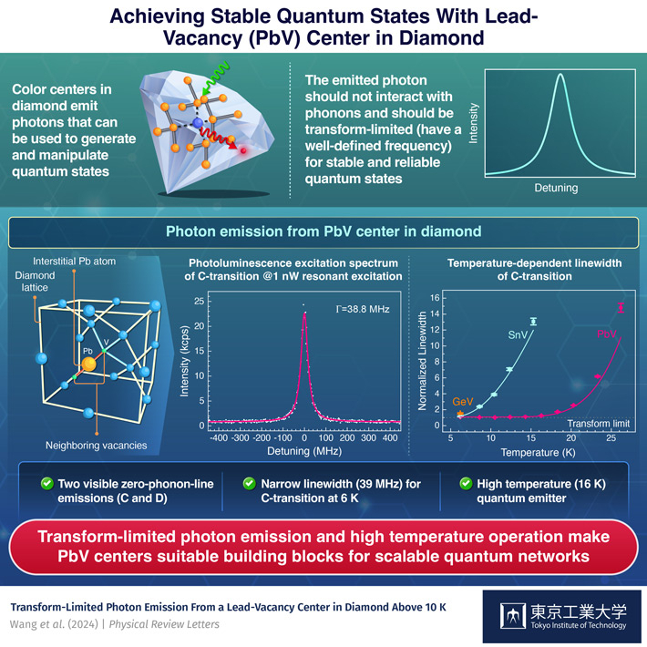
Much like how electric circuits use components to control electronic signals, quantum networks rely on special components and nodes to transfer quantum information between different points, forming the foundation for building quantum systems. In the case of quantum networks, color centers in diamond, which are defects intentionally added to a diamond crystal, are crucial for generating and maintaining stable quantum states over long distances.
When stimulated by external light, these color centers in diamond emit photons carrying information about their internal electronic states, especially the spin states. The interaction between the emitted photons and the spin states of the color centers enables quantum information to be transferred between different nodes in quantum networks.
A well-known example of color centers in diamond is the nitrogen-vacancy (NV) center, where a nitrogen atom is added adjacent to missing carbon atoms in the diamond lattice. However, the photons emitted from NV color centers do not have well-defined frequencies and are affected by interactions with the surrounding environment, making it challenging to maintain a stable quantum system.
To address this, an international group of researchers, including Associate Professor Takayuki Iwasaki from Tokyo Institute of Technology, has developed a single negatively charged lead-vacancy (PbV) center in diamond, where a lead atom is inserted between neighboring vacancies in a diamond crystal. In the study published in the journal Physical Review Letters![]() on February 15, 2024, the researchers reveal that the PbV center emits photons of specific frequencies that are not influenced by the crystal's vibrational energy. These characteristics make the photons dependable carriers of quantum information for large-scale quantum networks.
on February 15, 2024, the researchers reveal that the PbV center emits photons of specific frequencies that are not influenced by the crystal's vibrational energy. These characteristics make the photons dependable carriers of quantum information for large-scale quantum networks.
For stable and coherent quantum states, the emitted photon must be transform-limited, which means that it should have the minimum possible spread in its frequency. Additionally, it should have emission into zero-phonon-line (ZPL), meaning that the energy associated with the emission of photons is only used to change the electronic configuration of the quantum system, and not exchanged with the vibrational lattice modes (phonons) in the crystal lattice.
To fabricate the PbV center, the researchers introduced lead ions beneath the diamond surface through ion implantation. An annealing process was then carried out to repair any damage caused by the lead ion implantation. The resulting PbV center exhibits a spin 1/2 system, with four distinct energy states with the ground and the excited state split into two energy levels. On photoexciting the PbV center, electron transitions between the energy levels produced four distinct ZPLs, classified by the researchers as A, B, C, and D based on the decreasing energy of the associated transitions. Among these, the C transition was found to have a transform-limited linewidth of 36 MHz.
"We investigated the optical properties of single PbV centers under resonant excitation and demonstrated that the C-transition, one of the ZPLs, reaches the nearly transform-limit at 6.2 K without prominent phonon-induced relaxation and spectral diffusion," says Dr. Iwasaki.
The PbV center stands out by being able to maintain its linewidth at approximately 1.2 times the transform-limit at temperatures as high as 16 K. This is important to achieve around 80% visibility in two-photon interference. In contrast, color centers like SiV, GeV, and SnV need to be cooled to much lower temperatures (4 K to 6 K) for similar conditions. By generating well-defined photons at relatively high temperatures compared to other color centers, the PbV center can function as an efficient quantum light-matter interface, which enables quantum information to be carried long distances by photons via optical fibers.
"These results can pave the way for the PbV center to become a building block to construct large-scale quantum networks," concludes Dr. Iwasaki.
- Reference
| Authors : | Peng Wang1, Lev Kazak2, Katharina Senkalla2, Petr Siyushev2,3,4, Ryotaro Abe1, Takashi Taniguchi5, Shinobu Onoda6, Hiromitsu Kato7, Toshiharu Makino7, Mutsuko Hatano1, Fedor Jelezko2, and Takayuki Iwasaki1* |
|---|---|
| Title : | Transform-Limited Photon Emission From a Lead-Vacancy Center in Diamond Above 10 K |
| Journal : | Physical Review Letters |
| DOI : | 10.1103/PhysRevLett.132.073601 |
| Affiliations : | 1Department of Electrical and Electronic Engineering, School of Engineering, Tokyo Institute of Technology, Japan 2Institute for Quantum Optics, Ulm University, Germany 33rd Institute of Physics, University of Stuttgart, Germany 4Institute for Materials Research (IMO), Hasselt University, Belgium 5Research Center for Materials Nanoarchitectonics, National Institute for Materials Science, Japan 6Takasaki Advanced Radiation Research Institute, National Institutes for Quantum Science and Technology, Japan 7Advanced Power Electronics Research Center, National Institute of Advanced Industrial Science and Technology, Japan |
|
* Corresponding author's email: iwasaki.t.aj@m.titech.ac.jp |
|
- Breakthrough in Tin-Vacancy Centers for Quantum Network Applications | Tokyo Tech News
- High-accuracy Electric Vehicle Battery Monitoring with Diamond Quantum Sensors for Driving Range Extension Towards Carbon Neutrality | Tokyo Tech News
- Measuring Currents in the Heart at Millimeter Resolution with a Diamond Quantum Sensor | Tokyo Tech News
- How Flawed Diamonds "Lead" to Flawless Quantum Networks | Tokyo Tech News
- Artificially introduced atomic-level sensors enable measurements of the electric field within a working semiconductor device | Tokyo Tech News
- New diamond structures produce bright luminescence for quantum cryotography and biomarkers applications | Tokyo Tech News
- Quantum science and technology | Research Stories | Research
- Mutsuko Hatano - Diamonds as the ultimate semiconductors | Research Stories | Research
- Six Tokyo Tech faculty members receive FY2019 MEXT Commendation | Tokyo Tech News
- Takayuki Iwasaki | Researcher Finder - Tokyo Tech STAR Search
- Mutsuko Hatano | Researcher Finder - Tokyo Tech STAR Search
- Hatano & Iwasaki Lab.
- Energy Science and Informatics Graduate Major|Education|Department of Electrical and Electronic Engineering, School of Engineering
- Electrical and Electronic Engineering Graduate Major|Education|Department of Electrical and Electronic Engineering, School of Engineering
- Electrical and Electronic Engineering Undergraduate Major|Education|Department of Electrical and Electronic Engineering, School of Engineering
- Institute for Quantum Optics | Ulm University
- Research Center for Materials Nanoarchitectonics | MANA
- Advanced Power Electronics Research Center
- Latest Research News
School of Engineering
—Creating New Industries and Advancing Civilization—
Information on School of Engineering inaugurated in April 2016
Further Information
Associate Professor Takayuki Iwasaki
School of Engineering, Tokyo Institute of Technology

