Electrical and Electronic Engineering News
Tapping into the 300 GHz Band with an Innovative CMOS Transmitter
New phased-array transmitter design overcomes common problems of CMOS technology in the 300 GHz band, as reported by scientists from Tokyo Tech. Thanks to its remarkable area efficiency, low power consumption, and high data rate, the proposed transmitter could pave the way to many technological applications in the 300 GHz band, including body and cell monitoring, radar, 6G wireless communications, and terahertz sensors.
Today, most frequencies above the 250 GHz mark remain unallocated. Accordingly, many researchers are developing 300 GHz transmitters/receivers to capitalize on the low atmospheric absorption at these frequencies, as well as the potential for extremely high data rates that comes with it.
However, high-frequency electromagnetic waves become weaker at a fast pace when travelling through free space. To combat this problem, transmitters must compensate by achieving a large effective radiated power. While some interesting solutions have been proposed over the past few years, no 300 GHz-band transmitter manufactured via conventional CMOS processes has simultaneously realized high output power and small chip size.
Now, a research team led by Professor Kenichi Okada from Tokyo Institute of Technology (Tokyo Tech) and NTT Corporation (Headquarters: Chiyoda-ku, Tokyo; President & CEO: Akira Shimada; "NTT") have recently developed a 300 GHz-band transmitter that solves these issues through several key innovations. Their work was presented in the 2024 IEEE International Solid-State Circuits Conference (ISSCC)![]() .
.
The proposed solution is a phased-array transmitter composed of 64 radiating elements, which are arranged in 16 integrated circuits with four antennas each. Since the elements are arranged in three dimensions by stacking printed circuit boards (PCBs), this transmitter supports 2D beam steering. Simply put, the transmitted power can be aimed both vertically and horizontally, allowing for fast beam steering and tracking receivers efficiently. Notably, the antennas used are Vivaldi antennas, which can be implemented directly on-chip and have a suitable shape and emission profile for high frequencies.
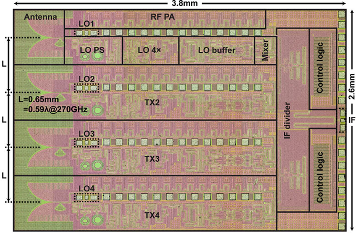
Figure 1. Chip die micrograph
- The proposed transmitter chip could pave the way for enhanced body and cell monitoring, radar, 6G wireless communications, and terahertz sensors.
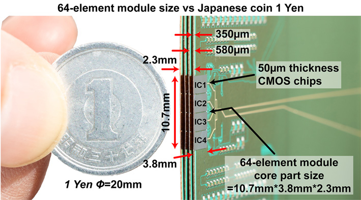
Figure 2. Compact phased-array transmitter with on-chip antennas
- Thanks to a highly optimized circuit topology and layout, the proposed transmitter chips can be arranged into a 64-element array occupying a minuscule volume.
An important feature of the proposed transmitter is its power amplifier (PA)-last architecture. By placing the amplification stage right before the antennas, the system only needs to amplify signals that have already been conditioned and processed. This leads to higher efficiency and better amplifier performance.
The researchers also addressed a few common problems that arise with conventional transistor layouts in CMOS processes, namely high gate resistance and large parasitic capacitances. They optimized their layout by adding additional drain paths and vias and by altering the geometry and element placing between metal layers. "Compared to the standard transistor layout, the parasitic resistance and capacitances in the proposed transistor layout are all mitigated," remarks Prof. Okada. "In turn, the transistor-gain corner frequency, which is the point where the transistor's amplification starts to decrease at higher frequencies, was increased from 250 to 300 GHz."
On top of these innovations, the team designed and implemented a multi-stage 300 GHz power amplifier to be used with each antenna. Thanks to excellent impedance matching between stages, the amplifiers demonstrated outstanding performance, as Prof. Okada highlights: "The proposed power amplifiers achieved a gain higher than 20 dB from 237 to 267 GHz, with a sharp cut-off frequency to suppress out-of-band undesired signals." The proposed amplifier also achieves a noise figure of 15 dB which was evaluated by the noise measurement system in 300-GHz band.
The researchers tested their design through both simulations and experiments, obtaining very promising results. Remarkably, the proposed transmitter achieved a data rate of 108 Gb/s in on-PCB probe measurements, which is substantially higher than other state-of-the-art 300 GHz-band transmitters.
Moreover, the transmitter also displayed remarkable area efficiency compared to other CMOS-based designs alongside low power consumption, highlighting its potential for miniaturized and power-constrained applications. Some notable use cases are sixth-generation (6G) wireless communications, high-resolution terahertz sensors, and human body and cell monitoring.
Make sure to stay tuned for future technological developments in the 300 GHz band!
- Reference
| Conference : | 2024 IEEE International Solid-State Circuits Conference (ISSCC) |
| Session : | Session 24 – D-Band/Sub-THz Transmitters and Sensors (February 21, 10:55AM, PST, local time) |
| Session Title : | A 236-to-266GHz 4-Element Amplifier-Last Phased-Array Transmitter in 65nm CMOS |
| Authors : | Chun Wang1, Hans Herdian1, Wenbin Zheng1, Chenxin Liu1, Jill Mayeda1, Yuxuan Liu1, Olivia Angel Yong1, Wenqian Wang1, Yuncheng Zhang1, Carrel da Gomez1, Abanob Shehata1, Sena Kato1, Ibrahim Abdo2, Teruo Jyo2, Hiroshi Hamada2, Hiroyuki Takahashi2, Hiroyuki Sakai1, Atsushi Shirane1, and Kenichi Okada1 |
| Affiliations : | 1Tokyo Institute of Technology, Japan 2Nippon Telegraph and Telephone, Japan |
- Combating Fractional Spurs in Phase Locked Loops to Improve Wireless System Performance in Beyond 5G | Tokyo Tech News
- World's First Successful High-Speed Data Transmission with Beamforming in 300 GHz Band | Tokyo Tech News
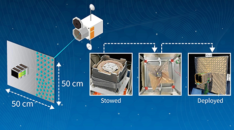
- Towards the New-Space Era with Foldable Phased-Array Transmitters for Small Satellites | Tokyo Tech News
- Preparing the Stage for 6G: A Fast and Compact Transceiver for Sub-THz Frequencies | Tokyo Tech News
- New Transmitter Design for Small Satellite Constellations Improves Signal Transmission | Tokyo Tech News
- Novel Architecture Can Reduce Noise-Induced Jitters in Digital Technology | Tokyo Tech News
- Improving the Performance of Satellites in Low Earth Orbit | Tokyo Tech News
- New and Improved Multi-Band Operational Receiver for 5G New Radio Communication | Tokyo Tech News
- Efficient Satellite Downlink with a Ka Band Dual Circular Polarization Transmitter | Tokyo Tech News
- Introducing a Transceiver that Can Tap into the Higher Frequency Bands of 5G Networks
- Electricity and Data Over-the-Air: The Simultaneous Transmission of 5G and Power | Tokyo Tech News
- Novel Fast-Beam-Switching Transceiver Takes 5G to the Next Level | Tokyo Tech News
- Lean and mean: Maximizing 5G communications with an energy-efficient relay network | Tokyo Tech News
- Pushed to the Limit: A CMOS-based transceiver for beyond 5G applications at 300 GHz | Tokyo Tech News
- Greater Connectedness in Remote Areas: A Ka-band Transceiver for Satellite Communications | Tokyo Tech News
- Researchers develop a compact 28-GHz transceiver supporting dual-polarized MIMO | Tokyo Tech News
- Smallest all-digital circuit opens doors to 5 nm next-gen semiconductor | Tokyo Tech News
- Three Tokyo Tech Faculty Members to Receive 2023 IEEE Fellow Titles | Tokyo Tech News
- Kenichi Okada - Wiring the world wirelessly | Research Stories | Research
- Kenichi Okada | Researcher Finder - Tokyo Tech STAR Search
- Hiroyuki Sakai | Researcher Finder - Tokyo Tech STAR Search
- Atsushi Shirane | Researcher Finder - Tokyo Tech STAR Search
- Okada Laboratory
- Electrical and Electronic Engineering Graduate Major|Education|Department of Electrical and Electronic Engineering, School of Engineering
- Electrical and Electronic Engineering Undergraduate Major|Education|Department of Electrical and Electronic Engineering, School of Engineering
- NTT / NTT Group | Nippon Telegraph and Telephone Corporation
- Latest Research News

School of Engineering
—Creating New Industries and Advancing Civilization—
Information on School of Engineering inaugurated in April 2016
Further Information
Professor Kenichi Okada
School of Engineering, Tokyo Institute of Technology
Email okada@ee.e.titech.ac.jp
Tel +81-3-5734-3764
Featured News

![]()