Electrical and Electronic Engineering News
World’s fastest directly modulated laser exceeding 100-GHz bandwidth
Membrane laser on silicon carbide substrate achieves low power consumption
Nippon Telegraph and Telephone Corporation (NTT), in collaboration with Fumio Koyama, professor at the Laboratory for Future Interdisciplinary Research of Science and Technology, Tokyo Institute of Technology, has developed an ultra-highspeed membrane laser[1] that uses an indium-phosphorus compound semiconductor[2] on a silicon carbide substrate[3] with high thermal conductivity. This laser, the world's first directly modulated laser with a 3-dB bandwidth[4] exceeding 100 GHz, can transmit at 256 gigabits (256 billion bits) per second over a distance of 2 km in a single-mode fiber.
Directly modulated lasers are now widely used in data center[5], but their modulation speed is limited, which has been a problem for further increasing in transmission capacity. These results will enable us to respond to the expected increase in traffic with a low-cost and low-power-consumption solution and will contribute to the realization of a high-capacity optical transmission infrastructure that supports NTT's IOWN[6] concept.
This research was reported in Nature Photonics on October 19, 2020.
Background to Research
Data traffic will continue to increase in the future, especially in data centers where data is concentrated. Therefore, it is essential to increase the capacity of optical interconnections[7] that connect servers. Moreover, the increase in power consumption in data centers must be suppressed, so it is important to reduce the power consumption of optical interconnects. Currently, directly modulated lasers are widely used in data centers because of their low power consumption and low cost. However, since they use intensity modulation, in which the light (photons[8]) output varies in proportion to the current (carrier[9]) injected into the laser, their modulation speed is limited by the relaxation oscillation frequency[10], which is the interaction between carriers and photons. Figure 1 shows the evolution of the 3-dB bandwidth for directly modulated lasers over the last 30 years. In the 1990s, the performance of the laser active layer[11] was improved, resulting in a 3-dB bandwidth of about 30 GHz, but no significant progress has been made since then.
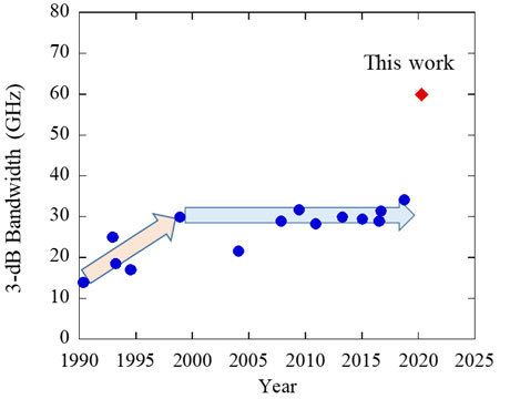
Figure 1. Trend in 3-dB bandwidth of DMLs.
Since further improving the performance of the active layer is considered to be difficult, photon-photon resonance has attracted attention as an additional speed-up method. In this method, when the frequency detuning between the lasing mode[12] and the adjacent cavity mode[13] coincides with a specific modulation frequency, the sideband[14] generated by the intensity modulation is enhanced. Figure 2 shows the change in the 3-dB bandwidth when photon-photon resonance is applied. Up to now, a 3-dB bandwidth of 55 GHz has been achieved, and PAM4 signal modulations[15] at 112 gigabits per second have been demonstrated.
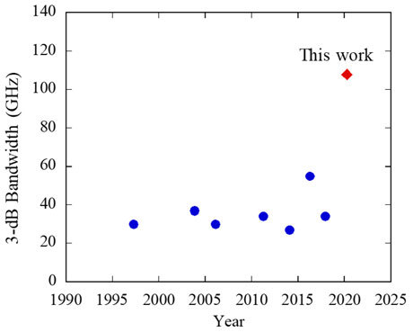
Figure 2. Trend in 3-dB bandwidth of DMLs using additional speed-up scheme.
Although it is possible to increase the response of a specific frequency by adjusting the detuning, it is necessary to have a flat frequency response characteristic from a low-frequency region to a high-frequency region for further speed-up. For this purpose, it is important to increase the relaxation oscillation frequency and prevent a large drop between the relaxation oscillation frequency and the photon-photon resonance frequency.
Research Results
To increase the relaxation oscillation frequency, NTT researchers focused on the optical confinement factor of the active region and developed a membrane laser on a silicon (Si) substrate with a thermal oxide film (SiO2). Membrane lasers have a large optical confinement factor in the active region and are compact, making it possible to realize directly modulated lasers with low power consumption. On the other hand, since the device is fabricated on a low-thermal-conductivity SiO2 layer, the temperature increase in the active layer due to current injection is large, and even if the current is increased, the relaxation oscillation frequency saturates at about 20 GHz due to saturation of the differential gain.
To suppress the increase in the active region temperature, we fabricated an indium-phosphorus (InP) based membrane laser on a silicon carbide (SiC) substrate (Fig. 3), which has a thermal conductivity approximately 500 times higher than that of SiO2. Since SiC has a lower refractive index than InP, the optical confinement factor is almost the same as that of the device on SiO2. The device was fabricated by direct bonding with ultrathin (40 nanometers) SiO2 between the InP and SiC substrate. Assuming a 100-mW heat source, the temperature increase in the active region of a membrane laser with an active layer length of 50 micrometers was significantly reduced from 130.9 to 16.8˚C when the SiO2 thickness was reduced from 2 micrometers to 40 nanometers (Fig. 4). The current at which the relaxation frequency reaches its maximum was 5.5 mA for the device fabricated on SiO2/Si substrate. In contrast, with the device fabricated on SiC substrate, we were able to increase the current to 30 mA and obtain the world's highest relaxation frequency of 42 GHz and 3-dB band of 60 GHz (Fig. 5).
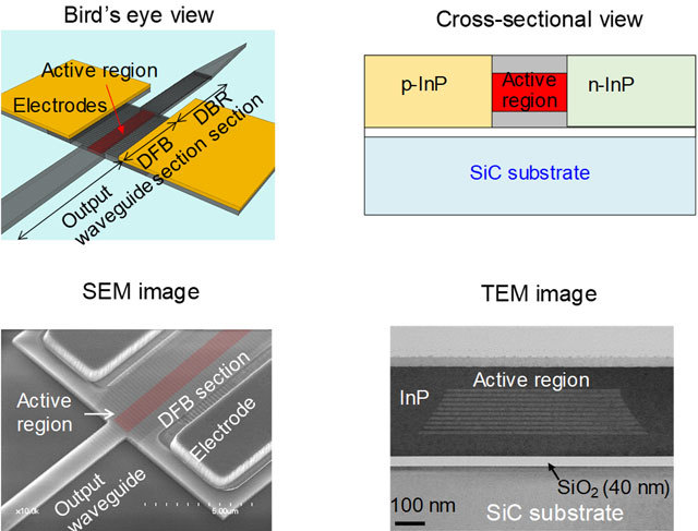
Figure 3. Schematic diagrams of device and SEM and TEM images of fabricated device.
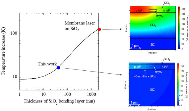
- Figure 4. Temperature increase in the active region of a membrane laser with an active layer length of 50 micrometers when we assume a 100-mW heat source.
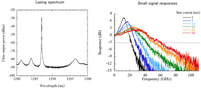
Figure 5. Lasing spectrum and small-signal responses of the device without reflection at the facet.
In addition, using optical feedback from the end facet of the output waveguide, we designed a device in which photon-photon resonance occurs at around 95 GHz. As a result, we obtained a 3-dB bandwidth of 108 GHz (Fig. 6) and succeeded in generating a 256 gigabit (256 billion bit) PAM4 signal and transmitting it over a distance of 2 km (Fig. 7).
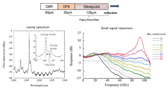
Figure 6. Lasing spectrum and small-signal responses of the device with reflection at the facet.
![Figure 7. Generation of 256 Gbit/s PAM-4 signal and bit error rate measurement results for back-to-back and 2-km transmission. At bit error rates below the dash-dotted line, data can be transferred without error using FEC[16].](/ee/eng/news/img/news_059772_07.jpg)
- Figure 7. Generation of 256 Gbit/s PAM-4 signal and bit error rate measurement results for back-to-back and 2-km transmission. At bit error rates below the dash-dotted line, data can be transferred without error using FEC[16].
Future Developments
The future will see the development of transmitters capable of handling the next generation of Ethernet standards with transmission capacity exceeding 1 terabit with four or eight arrays. The simultaneous achievement of low power consumption is expected to suppress increases in the power consumption of data centers and supercomputers due to the anticipated increase in data volume.
Technical Points
1. Membrane lasers on SiC substrate
As shown in Fig. 3, the membrane laser is a laser with total thickness of about 300 nm (1/10 that of conventional lasers) made on a low-refractive-index material. The active region is embedded in the InP layer, and a lateral current injection structure is formed. Since the membrane laser is sandwiched between low-refractive-index layers, light (photons) generated in the active region is strongly confined in it. In addition to this, since the injected carriers are also tightly confined in the active layer, low power consumption and high-speed modulation of direct modulation lasers can be expected. Figure 8 shows the optical mode field in membrane lasers on SiO2 and SiC. As shown in the figure, although SiC has about 500 times the thermal conductivity of SiO2, the optical confinement is similar.
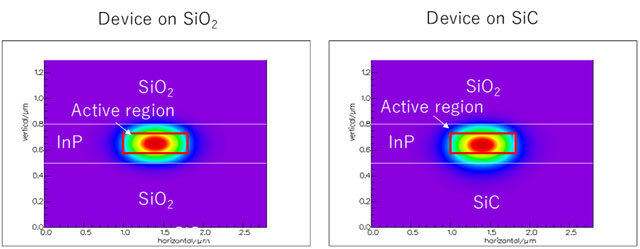
Figure 8. Optical mode fields of the devices on SiO2 and SiC.
2. Fabrication Method
SiC and InP are directly bonded to SiO2 using oxygen plasma. Although SiO2 provides good bonding strength, it is important to make it as thin as possible due to its low thermal conductivity. To prevent peeling of the film due to out-gas generated when the temperature rises after bonding, we succeeded in forming a groove in the substrate.
Figure 9 shows the fabrication process. First, the InP substrate is removed after direct bonding (a). Then, the active layer in the core region of the laser is left, and the active layer is etched away to the lower InP layer in other regions (b). InP is selectively regrown on the surface where the InP layer is exposed. This embeds the active layer into the InP layer (c). The device is then fabricated by selectively forming doping regions, gratings, and electrodes (d).
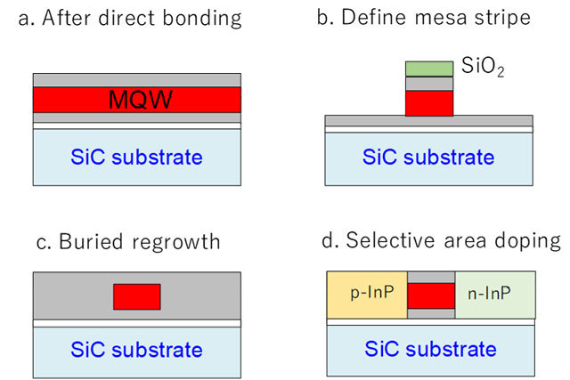
Figure 9. Fabrication procedure.
3. Design of cavity photon lifetime
When the relaxation oscillation frequency increases, the frequency response of the directly modulated laser is limited by the photon lifetime—the time that photons are confined in the cavity—and by the nonlinear saturation of the gain of the active layer. In this experiment, we focused on the photon lifetime. Figure 10 shows calculated frequency response characteristics when the photon lifetime in the cavity is changed. In the calculation, the relaxation oscillation frequency was kept constant at 40 GHz. As shown in the figure, the 3-dB bandwidth can be maximized by setting the photon lifetime at around one picosecond.
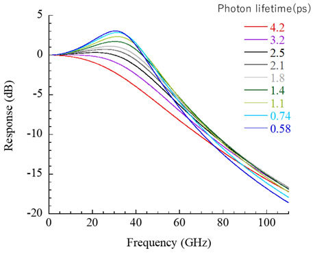
- Figure 10. Calculated frequency response characteristics when the photon lifetime in the cavity is changed. In the calculation, the relaxation oscillation frequency was kept constant at 40 GHz.
- Technical Terms
[1] Membrane laser : A thin-film laser surrounded by a low refractive index material such as air or SiO2
[2] Indium phosphorus compound semiconductor : A group III-V compound semiconductor containing indium and phosphorus. By mixing in an appropriate amounts of Ga (gallium), Al (aluminum), and As (arsenic), the operating wavelength of lasers, modulators, and photodetectors can be adjusted. It is also used to fabricate high-speed electronic circuits
[3] SiC substrate : Group IV compound semiconductor consisting of silicon (Si) and carbon (C). Thermal conductivity is 490 W/(m K); refractive index is 2.58. In addition to being widely used as a power semiconductor, it is used as a substrate to efficiently dissipate heat generated by lasers because of its high thermal conductivity.
[4] 3-dB bandwidth : In the frequency response characteristics of the device, the frequency at which the modulation amplitude decreases by 3 dB (in half) when the device is modulated from a low frequency to a high frequency.
[5] Data center : A facility that contains equipment such as servers that store data on the Internet and routers that control the communication between servers. With the progress of the Internet, huge data centers are required, and their power consumption becomes a problem.
[6] IOWN (Innovative Optical and Wireless Network) : Future communications infrastructure that utilizes cutting-edge optical and information processing technologies to realize a smart world.
[7] Optical interconnection : A method of connecting devices by converting electrical signals into optical signals, for which a semiconductor laser is used. By using optical fiber with low loss and high bandwidth, the signal can be transmitted and received with lower power consumption than signal transmission by the electricity.
[8] Photons : Particles of light emitted when electrons and holes recombine.
[9] Carriers : Electrons and holes generated by current injection or photoexcitation. Light is emitted when electrons and holes recombine.
[10] Relaxation oscillation frequency : When a pulsed current is injected into a laser, a large number of photons are generated, and laser oscillation occurs due to the rapid increase in carriers in the laser resonator. The photons in the cavity generate stimulated emission, resulting in carrier reduction. As the carriers decrease, the photons decrease, causing temporal variations in the optical output. The frequency of this oscillation is called the relaxation oscillation frequency, which is a major factor limiting the speed of direct modulation of the laser.
[11] Laser active layer : The region where carriers are injected and photons are generated. In indium phosphorus compound semiconductors, the emission wavelength of the laser is obtained by adjusting the content of Ga, Al, As, etc.
[12] Lasing Mode : The cavity mode in which the laser oscillates. A laser that oscillates selectively in only one cavity mode is called a single-mode laser.
[13] Cavity mode : In order to obtain laser oscillation, the phase of the light traveling around the resonator must match the initial value due to the nature of light as a wave. This matching wavelength is called the cavity mode.
[14] Sideband : When the laser is intensity-modulated at a certain frequency, the oscillation spectrum broadens. In this case, a peak that appears at a frequency difference corresponding to the modulation frequency is generated on the low-frequency side and high-frequency side.
[15] PAM (Pulse Amplitude Modulation) 4 signal : 4-level pulse amplitude modulation. An intensity modulation method that transmits 2-bit data (00, 01, 10, 11) as four analog level pulse signals.
[16] FEC (Forward Error Correction) : FEC adds a code on the sender side correct errors that occurs when transmitting data, and detects and corrects errors on the receiver side. As the number of codes to be added increases, the amount of data that can be error-corrected increases, but the cost increases. HD-FEC uses 7% of the total number of bits as the error correction code, and KP4-FEC uses 5.8%.
- Reference
| Authors : | Suguru Yamaoka1, Nikolaos-Panteleimon Diamantopoulos1, Hidetaka Nishi1, Ryo Nakao1, Takuro Fujii1, Koji Takeda1, Tatsurou Hiraki1, Takuma Tsurugaya1, Shigeru Kanazawa2, Hiromasa Tanobe2, Takaaki Kakitsuka1,4, Tai Tsuchizawa1, Fumio Koyama3 and Shinji Matsuo1 |
|---|---|
| Title of original paper : | Directly modulated membrane lasers with 108 GHz bandwidth on a high-thermal-conductivity silicon carbide substrate |
| Journal : | Nature Photonics |
| DOI : | 10.1038/s41566-020-00700-y |
| Affiliations : |
1 NTT Device Technology Labs, NTT Corporation, Atsugi-shi 2 NTT Device Innovation Center, NTT Corporation, Atsugi-shi 3 Laboratory for Future Interdisciplinary Research of Science and Technology, Tokyo Institute of Technology, Yokohama 4 Present address: Graduate School of Information, Production and Systems, Waseda University, Kitakyushu |
* Corresponding author's email: suguru.yamaoka.hm@hco.ntt.co.jp
- Institute of Innovative Research — A new vision for science and technology | Tokyo Tech Stories | About Tokyo Tech
- Fumio Koyama to receive 2019 Nick Holonyak, Jr. Award | Tokyo Tech News
- Fumio Koyama to receive 27th Okawa Prize | Tokyo Tech News
- Photonics Integration System Research Center (Koyama, Uenohara, Miyamoto Lab.)
- Researcher Profile | Tokyo Tech STAR Search - Fumio Koyama
- Institute of Innovative Research (IIR)
- Laboratory for Future Interdisciplinary Research of Science and Technology (FIRST)
- Electrical and Electronic Engineering Graduate Major|Education|Department of Electrical and Electronic Engineering, School of Engineering
- Nippon Telegraph and Telephone Corporation (NTT)
- Latest Research News
Further Information
Professor Fumio Koyama
Institute of Innovative Research,
Tokyo Institute of Technology
Email koyama@pi.titech.ac.jp
Featured News


![]()