Electrical and Electronic Engineering News
3D solutions to energy savings in silicon power transistors
Tokyo Tech researchers demonstrate operation energy-savings in a low price silicon power transistor structure by scaling down in all three dimensions.
In electronics, lower power consumption leads to operation cost savings, environmental benefits and the convenience advantages from longer running devices. While progress in energy efficiencies has been reported with alternative materials such as SiC and GaN, energy-savings in the standard inexpensive and widely used silicon devices are still keenly sought. K Tsutsui at Tokyo Institute of Technology and colleagues in Japan have now shown that by scaling down size parameters in all three dimensions their device they can achieve significant energy savings.
Tsutsui and colleagues studied silicon insulated gate bipolar transistors (IGBTs), a fast-operating switch that features in a number of every day appliances. While the efficiency of IGBTs is good, reducing the ON resistance, or the voltage from collector to emitter required for saturation (Vce(sat)), could help increase the energy efficiency of these devices further.
Previous investigations have highlighted that increases in the "injection enhancement (IE) effect", which give rise to more charge carriers, leads to a reduction in Vce(sat). Although this has been achieved by reducing the mesa width in the device structure, the mesa resistance was thereby increased as well. Reducing the mesa height could help counter the increased resistance but is prone to impeding the (IE) effect. Instead the researchers reduced the mesa width, gate length, and the oxide thickness in the MOSFET to increase the IE effect and so reduce Vce(sat) from 1.70 to 1.26 V. With these alterations the researchers also used a reduced gate voltage, which has advantages for CMOS integration.
They conclude, "It was experimentally confirmed for the first time that significant Vce(sat) reduction can be achieved by scaling the IGBT both in the lateral and vertical dimensions with a decrease in the gate voltage."
Background
Insulated gate bipolar transistors (IGBTs)
These are three terminal devices used as switches or rectifiers. With simple gate-drive characteristics and high-current and low-saturation-voltage capabilities they combine the benefits of two other types of transistors - metal-oxide-semiconductor field effect transistors (MOSFETs) and bipolar transistors.
3D scaling of IGBTs
The researchers reduced the mesa width, gate length, and the oxide thickness in the MOSFET by a factor of 1/k, and compared devices with values of 1 and 3 for k. Because the fabrication of narrow mesas can cause problems they also reduced the trench depth by 1/k. Although this has a slightly negative effect on the IE effect, it has considerable benefits for fabrication ease and cost and the dependence of (Vce(sat)) on the trench depth was deemed to be small. The gate voltage was also decreased by a factor of 1/k, while the cell pitch was maintained at 16 μm.
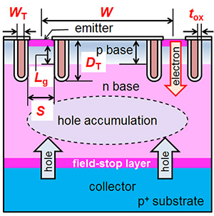
Figure. Trench gate IGBT schematic indicating the mesa width (S), gate length (Lg), and the oxide thickness in the MOSFET (tox), cell pitch (W), and the trench depth (DT).
Reference
| Authors : | K. Kakushima1, T. Hoshii1, K. Tsutsui1, A. Nakajima2, S. Nishizawa2, H. Wakabayashi1, I. Muneta1, K. Sato3, T. Matsudai4, W. Saito4, T. Saraya5, K. Itou5, M. Fukui5, S. Suzuki5, M. Kobayashi5, T. Takakura5, T. Hiramoto5, A. Ogura6, Y. Numasawa6, I. Omura7, H. Ohashi1, and H. Iwai1 |
|---|---|
| Title of original paper : | Experimental verification of a 3D scaling principle for low Vce(sat) IGBT, Technical Digest of IEDM2016, Session 10.6, (2016) 2016 IEEE International Electron Devices Meeting (IEDM) |
| Affiliations : | 1Laboratory for Future Interdisciplinary Research of Science and Technology, Tokyo Institute of of Technology, Yokohama, Japan 2Nat. Inst. Advanced Industrial Science and Technology, Tsukuba, Japan 3Mitusbishi Electric, Fukuoka, Japan 4Toshiba Corp., Tokyo, Japan 5The University of Tokyo, Tokyo, Japan 6Meiji University, Kawasaki, Japan 7Kyushu Inst. of Technology, Kitakyushu, Japan |
*corresponding author e-mail ktsutsui@ep.titech.ac.jp
- Tsutsui Laboratory (Japanese)
- Researcher Profile | Tokyo Tech STAR Search - Kazuo Tsutsui
- Laboratory for Future Interdisciplinary Research of Science and Technology (FIRST), Institute of Innovative Research (IIR)
- Institute of Innovative Research (IIR)
- Latest Research News
Further information
Professor Kazuo Tsutsui
Laboratory for Future Interdisciplinary Research of Science and Technology,
Institute of Innovative Research
Email ktsutsui@ep.titech.ac.jp
Tel +81-45-924-5462
