Electrical and Electronic Engineering News
Harnessing the potential of unexplored terahertz waves ― Associate Professor Yukio Kawano
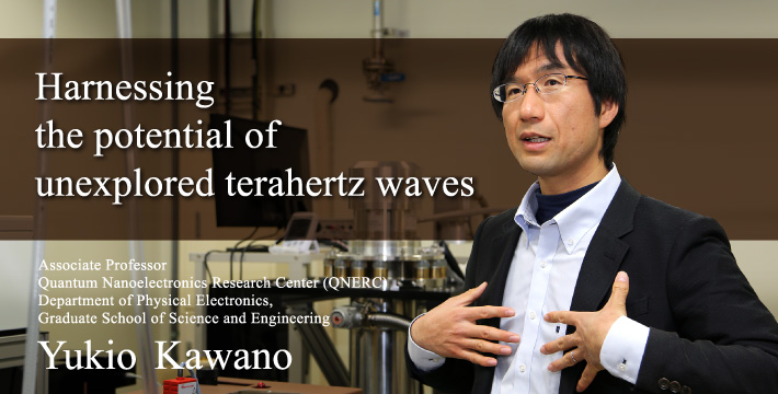
Exploring the last frontier of the electromagnetic spectrum
"While often thought of as very different, light and radio waves are both electromagnetic waves. What distinguishes the two is frequency."
This is how Associate Professor Yukio Kawano begins his introduction to terahertz waves. The terahertz is a unit of frequency for electromagnetic waves. Electromagnetic waves, formed by the vibrations of electric and magnetic fields, propagate through space and substance. These include gamma and X-rays with a wavelength shorter than light, and micro and radio waves with a longer wavelength.
Terahertz frequencies cover a range of about 1 THz between light and radio waves. Although the potential of terahertz technology has been suggested by research, it has long been considered a difficult area and not much work has been done in the field. As applications are now appearing, however, it is again attracting more interest.
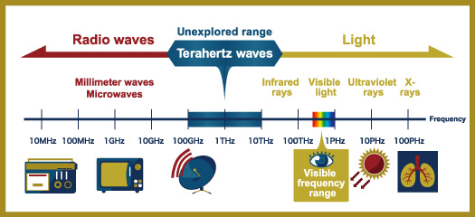
Figure 1. Terahertz frequency range
Terahertz waves exhibit great variability-they are permeable like radio waves and travel in straight lines like lasers. Since terahertz waves penetrate materials such as paper, wood, and plastic, images according to the rate of permeability of substances can be obtained. Using the shapes of these images, non-contact identification of substances is possible. Due to their rectilinear propagation, terahertz waves can also be reflected by a mirror and focused by a lens. In addition, when terahertz waves are irradiated to substances, they resonate with (crystalline) semiconductor lattice and biopolymer vibrations and absorb electromagnetic energy in chemical substances. In consequence, substance-specific spectra occur. Different chemical substances display different spectral characteristics, making it possible to identify impurities in pharmaceutical products in a non-destructive way. Other potential applications include the inspection of semiconductors and IC cards for quality control, preventing food contamination, monitoring water levels in flora, testing for toxic materials, inspecting historical items such as paintings or paper money to facilitate restoration or detect forgery, and pathology testing to detect cancer cells.
Terahertz development and application, however, has always been inhibited by two major obstacles. One is low image resolution. Images are created by exposing objects to light and radio waves. Shorter wavelengths produce greater detail, which increases resolution. Longer wavelengths, however, deliver low resolution. Terahertz wavelengths are longer than light, making images coarser. The other obstacle has been the lack of detectors compatible with terahertz radiation. Terahertz photon energy is too low to measure as light and too high to measure as radio waves, which means extremely low detection sensitivity. Measuring terahertz requires maximization of output involving an extremely large system. It is these two obstacles Kawano set out to overcome.
Nano-carbon miniaturizes detection and spectrometer devices
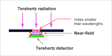
Figure 2. Terahertz detection setup
Kawano tried to increase image resolution to facilitate measurement. He installed a mechanism that generates a small amount of near-field light by irradiating terahertz radiation into holes that are smaller than wavelengths, and added a detector function into an all-in-one semiconductor chip. This increased resolution from 100 micrometers[1] to 400 nanometers[2] (1/540 of a wavelength), making it possible to measure fields smaller than wavelengths.
Next, Kawano developed a compact spectroscopic device capable of monitoring a broader frequency band. He used graphene, a material for which Andre Geim and Konstantin Novoselov received the Nobel Prize in Physics in 2010. Graphene allowed Kawano to increase the detection frequency from 0.76 to 33 THz, making broadband measurement possible. In 2014, Kawano worked with Rice University and Sandia National Laboratories in the US to jointly develop a terahertz detector employing a carbon nanotube array.
"Graphene is a honeycomb lattice of carbon atoms. Theoretically, the electron mass is zero. The electron speed is 1/300 that of light, which is exponentially faster than other materials. A carbon nanotube is one-dimensional linear material that detects oscillations in the terahertz radiation field while ignoring vibrations perpendicular to the nanotube."
Terahertz detectors also need to be cool for increased sensitivity. To solve this issue, Kawano utilized a carbon nanotube array in the detector. This innovation made use at room temperature possible and has been very highly regarded.
Curiosity led to exploration of a different area - Semiconductors
Kawano took his undergraduate and graduate degrees at the University of Tokyo. He continued his study of semiconductor physics, most notably the quantum Hall effect[3] , after becoming an assistant professor at his alma mater. He was interested in terahertz waves, but wanted to know about semiconductors as he felt that high resolution terahertz measurement could possibly contribute to the visual-control of semiconductor structure. At the time, however, his focus was still on the basics of semiconductors.
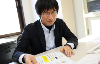
He moved to RIKEN and started working on terahertz waves. "RIKEN was excellent because there were no walls between research fields," says Kawano. RIKEN provides a free environment for researchers to engage in interdisciplinary studies. All researchers are encouraged to contact and seek knowledge from scientists in different fields. With his desire to explore the potential of semiconductor physics, Kawano realized that terahertz waves might be a tool for research. With this realization, he began focusing on terahertz development and application.
He moved to Tokyo Tech in 2011 and broadened his studies to include terahertz application to biotechnology and other industries through joint research with private companies. He has also continued his work on single-molecule measurement and other fundamental studies.
"Research on the future application of terahertz waves in observing and controlling the quantum state in solid matter and the characteristics of electron waves is progressing."
The presence of terahertz radiation in electron wave interference destroys the characteristics of an interference pattern. If we can restore it to its original state, we can control it. Kawano's studies have already achieved results that have brought him one step closer to this goal.
There are a number of problems to be solved before commercialization. The cost of producing measurement devices, for example, is a factor. If costs remain high, the technology will not be practical. Reducing the cost of the femtosecond[4] laser remains a challenge. It requires the development of a high-sensitivity low-noise semiconductor detector which utilizes mass-produced semiconductor chips.
It is also necessary to improve the power of the oscillator and increase the sensitivity of the detector. Many researchers around the world are working on the development of oscillators. At Tokyo Tech, Professor Masahiro Asada has taken the initiative in oscillator research and development.
Link between science and engineering
Since childhood, Kawano has been an avid reader with a wide range of interests, including classical literature. He even thought about pursuing the humanities. He tends to consider things without separating them into categories. As he shifted from the field of science to engineering at RIKEN, he was merely following his interests. This led him to results. Kawano looked back on what brought him to where he is now.
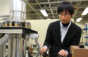
"My experience has shown me that science and engineering are linked. Therefore, I believe that collaboration across academic fields to deepen one's own fields of research and discover new areas contributes to the future development of science. I hope that all Tokyo Tech students will first concentrate on expanding the fundamental elements of their individual research. If they do this, their potential is unlimited."
Explanations of Technical Terms
1. Micrometer
One micrometer is 10-6 meters, 1 millionth of a meter, or 0.001 millimeters.
2. Nanometer
One nanometer is 10-9 meters, 1 billionth of a meter, or 0.000001 millimeters.
3. Quantum Hall effect
The quantum Hall effect is a phenomenon in which the longitudinal resistance of a two-dimensional electron system, created by confining electrons in a plane, such as at the different joint interfaces of semiconductors, becomes zero at low temperatures and in strong magnetic fields, under which Hall resistance is quantized. Nobel Prizes in Physics were awarded in 1985 and 1998 for the results of research on the quantum Hall effect.
4. Femtosecond
1 femtosecond is 10-15 seconds (1 quadrillionth of a second).
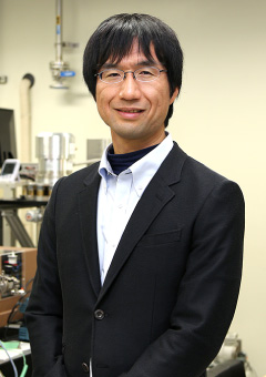
Yukio Kawano
Profile
- 2011Associate Professor of the Quantum Nanoelectronics Research Center (QNERC), and the Department of Physical Electronics in the Graduate School of Science and Engineering, Tokyo Institute of Technology
- 2009Senior Research Scientist, RIKEN
- 2006Research Scientist, RIKEN
- 2001Assistant Professor, Department of Physics, Graduate School of Science, University of Tokyo
- 2001Doctor of Science, Department of Multi-Disciplinary Sciences, Graduate School of Arts and Sciences, University of Tokyo
- 2000Research Fellow, Japan Society for the Promotion of Science (JSPS)
- 1998Master of Science, Department of Multi-Disciplinary Sciences, Graduate School of Arts and Sciences, University of Tokyo
- 1996Bachelor of Science, Department of Basic Science, College of Arts and Sciences, University of Tokyo
- 1974Born in Fukuoka
*This is an article originally featured on the Tokyo Tech website's top page![]() in May 2015.
in May 2015.
