Electrical and Electronic Engineering News
Lasers on silicon: Low temperature heterogeneous integration without glue
Realization of large scale photonic integration for one-chip optical routers is crucial for future optical networks and interconnection for big data transmission and artificial intelligence technology. To meet these technical needs, platforms based on silicon photonic integrated circuits are expected to play an important role because of the availability of large diameter wafers and CMOS fabrication technology.
However, it is difficult to realize light sources using silicon because it is an indirect bandgap semiconductor.
Now, Nobuhiko Nishiyama and colleagues at Tokyo Institute of Technology have demonstrated the operation of 1.55-μm GaInAsP lasers on silicon using low temperature plasma activated bonding (PAB).
The hybrid wafers, which consist of an InP-based wafer and a SOI wafer, were fabricated by PAB. The two wafers were irradiated with plasma in a vacuum chamber to active the surface. Then, the two wafers were bonded at 150 oC, which is much lower than that of conventional bonding methods. Even at such low temperature bonding, the wafers had sufficient bonding strength.
The hybrid lasers showed lasing operation at room temperature. The threshold current was 64 mA, which corresponds to a threshold current density of 850 A/cm2.
These hybrid lasers fabricated by low temperature bonding are expected to be a key technology to establish large scale photonic platforms.
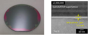
Figure 1. Optical microscope and SEM images of GaInAsP/SOI hybrid wafers.
Reference
| Authors | Yusuke Hayashi, Ryo Osabe, Keita Fukuda, Yuki Atsumi, JoonHyun Kang, Nobuhiko Nishiyama and Shigehisa Arai |
|---|---|
| Title of original paper | Low Threshold Current Density Operation of a GaInAsP/Si Hybrid Laser Prepared by Low-Temperature N2 Plasma Activated Bonding |
| Journal, volume, pages and year | Japanese Journal of Applied Physics, 52, 060202 (2013). |
| DOI | 10.7567/JJAP.52.060202 |
School of Engineering
—Creating New Industries and Advancing Civilization—
Information on School of Engineering inaugurated in April 2016
Further information
Associate Professor Nobuhiko Nishiyama
Department of Electrical and Electronic Engineering,
School of Engineering
Email nishiyama@ee.e.titech.ac.jp
Tel +81-3-5734-3593
Featured News

![]()