Electrical and Electronic Engineering News
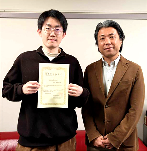
Outstanding Master Student Award in 2025! - Haiyun GU (Okada-Lab.)
In the 2025 academic year, out of 124 students in the Electrical and Electronic Engineering course (9 graduating in September, 115 in March), 10 students received this award for their outstanding master's thesis presentations. Here are interviews with the award recipients.
About my research
With the rapid development of Beyond 5G and 6G communication systems, wireless transceivers are required to support wide dynamic range signals while maintaining high linearity and low power consumption. In such systems, variable gain amplifiers (VGAs) play a crucial role in adjusting signal levels and ensuring stable receiver performance.
However, conventional VGA designs often suffer from trade-offs between linearity, noise performance, and gain control range. Especially in wideband RF systems, achieving fine and stable gain control without degrading signal quality remains a significant challenge.
This research focuses on a time-modulated CMOS variable gain amplifier (VGA) architecture. Instead of relying solely on traditional analog bias control, the proposed approach utilizes time-domain modulation to control the effective gain. By adjusting the duty cycle of the modulation signal, flexible and wide-range gain control can be achieved while maintaining high linearity.
The proposed design enables a wide dynamic gain range with minimal impact on signal distortion. In addition, the time-modulation approach offers a compact and power-efficient solution compared to conventional techniques, making it suitable for next-generation RF front-end systems.
One of the main challenges in this research was understanding and optimizing the impact of time-domain modulation on signal integrity, including noise and spectral characteristics. Through theoretical analysis and circuit simulations, the relationship between duty cycle, gain, and signal-to-noise ratio was clarified. Discussions within the laboratory also played an important role in refining the design and validating its effectiveness.
Comments on the award
I am deeply honored to receive the Outstanding Master Student Award in 2025. I would like to express my sincere gratitude to my supervisor, Professor Kenichi Okada, as well as to all the professors and members of the laboratory for their continuous support and guidance.
My experience in the Okada Laboratory has been both challenging and fulfilling. Through this research, I have strengthened my understanding of RF circuit design and developed a deeper appreciation for solving complex engineering problems. I hope to build upon this experience and continue contributing to the advancement of wireless communication technologies in the future.
Featured News


![]()