Chemical Science and Engineering News
Can't get thinner than this: synthesis of atomically flat boron sheets
Scientists at Tokyo Institute of Technology (Tokyo Tech) find a simple method for producing atomically thin layers of oxidized borophene, a promising 2D boron-based nanomaterial that could serve in a variety of fields.
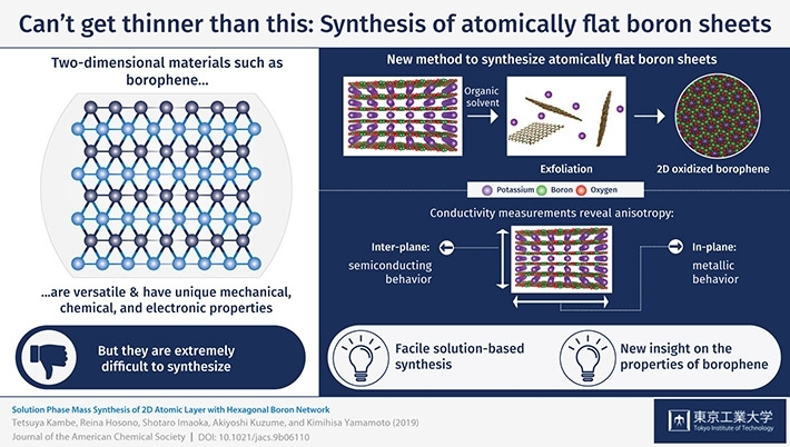
Since its rediscovery and characterization in 2004, graphene has been the focus of countless research efforts across multiple fields. It is a very versatile material consisting of a two-dimensional (2D) carbon network; in other words, it comprises a thin sheet of carbon that has a thickness of one atom. Graphene is not only stronger than the strongest steels, but also has a myriad of interesting chemical, electronic, and mechanical characteristics that has left scientists wondering if similar 2D networks of other materials could have such useful properties.
One novel 2D material that was recently reported is borophene, an analogue of graphene but consisting of boron atoms instead of carbon atoms. However, as one would expect for 2D sheets of any material, the synthesis of borophene has proved to be challenging. Researchers either require the use of a substrate to make borophene more stable or coupling boron with hydroxyl groups (OH-), which causes the structure to not be atomically flat.
In a recent study conducted at Tokyo Institute of Technology, a research team including Tetsuya Kambe, Akiyoshi Kuzume and Kimihisa Yamamoto was successful in synthesizing atomically flat oxidized borophene sheets through a simple solution-based method. First, they synthesized stacked layers of borophene oxide through a fairly simple process using a potassium borohydride salt (KBH4). An X-ray analysis revealed the 2D-layered structure of the material, in which layers of boron atoms forming a hexagonal 2D network with oxygen atoms as bridges were intercalated with layers containing potassium atoms. Then, the subsequent necessary step was to find a way to exfoliate atomically thin layers of the borophene oxide network. The researchers achieved this by putting the material in dimethylformamide, which is a commonly used organic solvent. Various types of measurements were carried out to verify the structure of the exfoliated sheets, including electron microscopy, spectroscopy, and atomic force microscopy. The results confirmed that the proposed method was effective for producing the desired atomically flat oxidized borophene sheets.
Finally, the researchers performed resistivity measurements to analyze the conducting properties of stacked borophene sheets and found an interesting characteristic referred to as anisotropy. This means that the sheets exhibited different types of conductivity depending on the direction of the current flow. The material behaved like a semiconductor in the inter-plane direction, whereas it exhibited metal-like behavior in the in-plane direction of the boron network. The mechanisms behind these two types of conducting behaviors were elucidated as well. "It is important to note that our boron sheets can be handled easily at ambient conditions," remarks Dr. Kambe, indicating that this pioneering research could be the basis for finding potential applications for borophene.
Finding facile methods for the synthesis of borophene and borophene-based compounds is crucial to conducting further research on this interesting material and its potential uses. "Like graphene, borophene is expected to have unique properties, including extraordinary mechanical characteristics and metallic behavior that could be exploited in a variety of fields," states Dr. Kambe. Hopefully, future findings and developments on 2D materials will enable us to employ their exotic properties and tailor them to suit our needs.
- Reference
| Authors : | Tetsuya Kambe1,2, Reina Hosono1, Shotaro Imaoka1, Akiyoshi Kuzume2, and Kimihisa Yamamoto1,2 |
|---|---|
| Title of original paper : | Solution Phase Mass Synthesis of 2D Atomic Layer with Hexagonal Boron Network |
| Journal : | Journal of the American Chemical Society |
| DOI : | 10.1021/jacs.9b06110 |
| Affiliations : |
1Laboratory for Chemistry and Life Science, Tokyo Institute of Technology 2JST-ERATO, Tokyo Institute of Technology |
- Breakthrough in blending metals: Precise control of multimetallic one-nanometer cluster formation achieved | Tokyo Tech News
- How a tetrahedral substance can be more symmetrical than a spherical atom | Tokyo Tech News
- Metallic nano-particles light up another path towards eco-friendly catalysts | Tokyo Tech News
- One-Nanometer Trimetallic Alloy Particles Created | Tokyo Tech News
- New aspect of atom mimicry for nanotechnology applications | Tokyo Tech News
- Controllable light-emitting materials to advance light sensing and nano-medicine | Tokyo Tech News
- YAMAMOTO-IMAOKA Group
- Researcher Profile | Tokyo Tech STAR Search - Tetsuya Kambe
- Researcher Profile | Tokyo Tech STAR Search - Kimihisa Yamamoto
- Institute of Innovative Research (IIR)
- Latest Research News
Further Information
Assistant Professor Tetsuya Kambe
Institute of Innovative Research
Email kambe@res.titech.ac.jp
Tel +81-45-924-5259
