Materials Science and Engineering News
Breakthrough in Semiconductor Patterning: New Block Copolymer Achieves 7.6 nm Line Width
A recently developed block copolymer could help push the limits of integration and miniaturization in semiconductor manufacturing, report scientists in Tokyo Tech and TOK. Chemically tailored for reliable directed self-assembly, the proposed compound can arrange itself into perpendicular lamellar structures whose half-pitch width is less than 10 nanometers, outperforming conventional and widely used block copolymers.
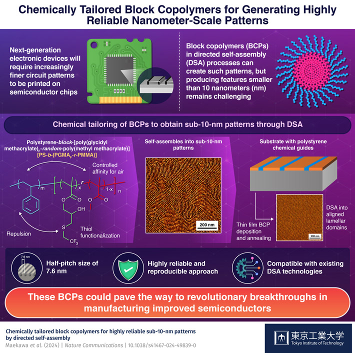
Miniaturization is one of the fundamental qualities of modern electronics and is largely responsible for the incredible increments in performance witnessed over the past decades. To keep this momentum going, it is necessary to achieve circuit patterns finer than the existing ones on semiconductor chips, which are a crucial part of all electronic devices. Some experts estimate that, by 2037, the smallest distance between features in semiconductor devices, known as 'half-pitch,' will need to be as small as 8 nm to support next-generation electronics, emphasizing the need for advancements in lithographic processes (method of creating highly complex circuit patterns on semiconductor parts).
As one would expect, creating such finely detailed structures on any kind of material is a massive undertaking. One promising avenue to achieve this feat is called directed self-assembly (DSA) with block copolymers (BCPs). Simply put, BCPs are long chain-like molecules made from two or more distinct sections—or blocks— of polymers. The process of DSA involves exploiting the interactions between different blocks in BCPs so that they spontaneously and consistently arrange themselves into ordered structures and patterns. While this strategy is certainly powerful, producing features smaller than 10 nanometers (sub-10 nm) using DSA remains challenging.
In a recent study published on 06 July 2024 in Nature Communications![]() , researchers from Tokyo Institute of Technology (Tokyo Tech) and Tokyo Ohka Kogyo (TOK) managed to push the envelope of the possibilities in this field. Led by Professor Teruaki Hayakawa, the research team developed a novel BCP that was carefully adapted to create incredibly small line patterns on a substrate in the form of lamellar domains (structure composed of fine and alternative layers). These tiny patterns could pave the way for new advanced semiconductor devices.
, researchers from Tokyo Institute of Technology (Tokyo Tech) and Tokyo Ohka Kogyo (TOK) managed to push the envelope of the possibilities in this field. Led by Professor Teruaki Hayakawa, the research team developed a novel BCP that was carefully adapted to create incredibly small line patterns on a substrate in the form of lamellar domains (structure composed of fine and alternative layers). These tiny patterns could pave the way for new advanced semiconductor devices.
The newly developed BCP was created from polystyrene-block-poly (methyl methacrylate) (or PS-b-PMMA), a representative and widely studied BCP for DSA. First, the researchers introduced an appropriate amount of poly (glycidyl methacrylate) (PGMA) into PS-b-PMMA, obtaining PS-b-(PGMA-r-PMMA). Afterwards, they modified the PGMA segment with different thiols, aiming to refine the repulsive interactions between the different blocks in the resulting polymer, named PS-b-PGFM. The PS and PMMA segments also controlled the affinity of the different parts of the molecule for air, which plays an important role in its self-alignment process during DSA.
The tailored BCP reliably self-assembled into exceptionally small nanometric lamellar structures when applied as a thin film, as confirmed by atomic force microscopy. Moreover, this new compound displayed impressive performance on a substrate with parallel polystyrene chemical guides.
"Thin-film aligned lamellar domains with a vertical orientation could be reliably and reproducibly obtained via directed self-assembly, yielding parallel line patterns that correspond to a half-pitch size of 7.6 nm," highlights Hayakawa. It is worth mentioning that this is one of the smallest half-pitch sizes reported worldwide for thin-film lamellar structures without a top coating.
Overall, these exciting findings have the potential to advance cutting-edge technologies in semiconductor manufacturing. "PS-b-PGFM BCPs are promising templates for use in lithography because they can produce fine patterns in DSA processes similar to the ones used for conventional PS-b-PMMA, with the potential to outperform them," concludes Hayakawa. "Studies aimed at optimizing the pattern-transfer processes using line patterns in PS-b-PGFM thin films as templates will be investigated in the future," he adds, sharing their objective for the future.
These advancements may bring us closer to a new era in electronics and artificial intelligence systems!
- Reference
| Authors : | Shinsuke Maekawa1, Takehiro Seshimo2, Takahiro Dazai2, Kazufumi Sato2, Kan Hatakeyama-Sato1, Yuta Nabae1, and Teruaki Hayakawa1 |
|---|---|
| Title : | Chemically tailored block copolymers for highly reliable sub-10-nm patterns by directed self-assembly |
| Journal : | Nature Communications |
| DOI : | 10.1038/s41467-024-49839-0 |
| Affiliations : | 1Department of Materials Science and Engineering, School of Materials and Chemical Technology, Tokyo Institute of Technology, Japan 2Research & Development Department, Tokyo Ohka Kogyo Co., Ltd., Japan |
|
* Corresponding author's email: hayakawa.t.ac@m.titech.ac.jp |
|
- Teruaki Hayakawa | Researcher Finder - Tokyo Tech STAR Search
- Kan Hatakeyama | Researcher Finder - Tokyo Tech STAR Search
- Yuta Nabae | Researcher Finder - Tokyo Tech STAR Search
- Hayakawa & Nabae Laboratory
- Nabae Laboratory
- Teruaki Hayakawa Laboratory | School of Materials and Chemical Technology Laboratory Search Site
- Materials Science and Engineering Graduate Major|Education|Department of Materials Science and Engineering, School of Materials and Chemical Technology
- Energy Science and Informatics Graduate Major |Education|Department of Materials Science and Engineering, School of Materials and Chemical Technology
- Materials Science and Engineering Graduate Major|Education|Department of Materials Science and Engineering, School of Materials and Chemical Technology
- Tokyo Ohka Kogyo Co., Ltd.
- Latest Research News
School of Materials and Chemical Technology
—Encompassing the Disciplines of Science—
Information on School of Materials and Chemical Technology inaugurated in April 2016
Further Information
Professor Teruaki Hayakawa
School of Materials and Chemical Technology,
Tokyo Institute of Technology
Email hayakawa.t.ac@m.titech.ac.jp
Tel +81-3-5734-2421

