Materials Science and Engineering News
Making Metal–Halide Perovskites Useful in Planar Devices Through a New Hybrid Structure
Two of the main drawbacks of using tin (Sn)-based metal halide perovskites (MHPs) in thin-film transistors have been simultaneously solved by an innovative hybrid 2D/3D structure proposed by scientists at Tokyo Institute of Technology (Tokyo Tech). Their findings will help unlock the potential of environmentally benign Sn-based MHPs in CMOS technology, paving the way for flexible and printable electronic devices.
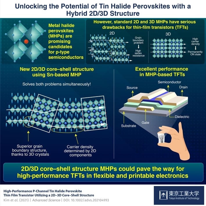
Metal halide perovskites (MHPs) are a class of materials with promising properties for semiconductor applications, such as thin-film transistors (TFTs). In particular, tin (Sn)-based MHPs could be an environmentally benign alternative to lead-based ones, which are toxic. However, some critical issues need to be resolved before Sn-based MHPs can be leveraged in planar semiconductor devices.
When arranged into a 2D structure (or quasi-2D structure with a few layers), defects in the crystal structure of Sn-based MHPs called "grain boundaries" hamper the mobility of charge carriers throughout the material. If used in a TFT, this phenomenon results in a large series resistance that ultimately degrades performance. In contrast, a TFT made using an Sn-based MHP arranged into a 3D structure faces a different yet still crippling problem. The extremely high carrier density of the 3D material causes the transistor to be permanently ON unless very high voltages are applied. Needless to say, this renders such a device useless for many applications.
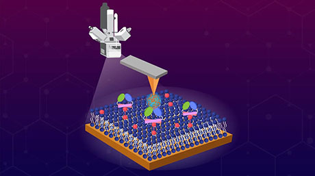
Fortunately, a team of scientists from Tokyo Tech, Japan, have found a solution to these limitations. In a recent study published in Advanced Science![]() and led by Assistant Professor Junghwan Kim and Honorary Professor Hideo Hosono, the researchers proposed a novel concept based on a hybrid structure for Sn-based MHPs, called the "2D/3D core–shell structure." In this structure, 3D MHP cores are fully isolated from one another and connected only through short 2D MHP strips (or "shells"). This alternating arrangement solves both of the abovementioned drawbacks simultaneously. But how?
and led by Assistant Professor Junghwan Kim and Honorary Professor Hideo Hosono, the researchers proposed a novel concept based on a hybrid structure for Sn-based MHPs, called the "2D/3D core–shell structure." In this structure, 3D MHP cores are fully isolated from one another and connected only through short 2D MHP strips (or "shells"). This alternating arrangement solves both of the abovementioned drawbacks simultaneously. But how?
The trick to lowering the series resistance of 2D MHPs is to eliminate the carrier mobility problems at grain boundaries, which are caused by misalignments between the conductive octahedra of the perovskite. Thanks to the way in which the 3D cores connect to the 2D segments, these misalignments disappear and the series resistance is greatly lowered. As for the high carrier density of 3D MHPs, this problem is simply not present when using the 2D/3D core–shell structure. Since the 3D cores are isolated, their carrier density is no longer relevant; instead, the 2D segments act as a bottleneck and limit the effective carrier density of the overall material.
To demonstrate the effectiveness of this novel structure, the team fabricated a complementary metal–oxide–semiconductor (CMOS) inverter by combining 2D/3D TFTs with a standard indium gallium zinc oxide TFT. "Our device exhibited a high voltage gain of 200 V/V at a drain voltage of 20 V. This performance is the best reported so far for a CMOS inverter made using Sn-MHP TFTs," highlights Prof. Kim.
The innovative 2D/3D structure presented in this study will help scientists worldwide take advantage of the attractive electronic properties of perovskites. Moreover, their approach is not limited to a narrow class of materials or device types. "The proposed strategy could be applied to various solution-derived semiconductor systems, opening doors to flexible and printable electronics," says Prof. Kim.
Only time will tell what technological innovations are unlocked by the findings of this study!
- Reference
| Authors : | Junghwan Kim1*, Yu-Shien Shiah1, Kihyung Sim1, Soshi Iimura2, Katsumi Abe3, Masatake Tsuji1, Masato Sasase1, and Hideo Hosono1,2* |
|---|---|
| Title of original paper : | High-Performance P-Channel Tin Halide Perovskite Thin Film Transistor Utilizing a 2D–3D Core–Shell Structure |
| Journal : | Advanced Science |
| DOI : | 10.1002/advs.202104993 |
| Affiliations : |
1 Materials Research Center for Element Strategy, Tokyo Institute of Technology 2 WPI-MANA, National Institute for Materials Science 3 Silvaco Japan Co., Ltd. |
* Corresponding authors' emails: JH.KIM@mces.titech.ac.jp (J. Kim); hosono@msl.titech.ac.jp (H. Hosono)
- Scientists Observe Record High Hydride Ion Conductivity Using Modified Lanthanum Trihydride | Tokyo Tech News
- Fabricating Stable, High-mobility Transistors for Next-generation Display Technologies | Tokyo Tech News
- Shedding Light on the Development of Efficient Blue-Emitting Semiconductors | Tokyo Tech News
- New design strategy brightens up the future of perovskite-based light-emitting diodes | Tokyo Tech News
- A low-voltage high-luminance perovskite LED realized — press event held | Tokyo Tech News
- Lighting it up: A new non-toxic, cheap, and stable blue photoluminescent material | Tokyo Tech News
- Hideo Hosono's story of IGZO TFT development features in Nature Electronics | Tokyo Tech News
- Research group at Tokyo Tech develops new material for the electron injection layer and transport layer of organic EL displays | Tokyo Tech News
- Hideo Hosono - Manipulating electrons well to elicit the potential of materials, Part 1 | Research Stories | Research
- Hideo Hosono - Manipulating electrons well to elicit the potential of materials, Part 2 | Research Stories | Research
- Professor Hideo Hosono receives 2016 Japan Prize | Tokyo Tech News
- Junghwan Kim | Researcher Finder - Tokyo Tech STAR Search
- Hideo Hosono | Researcher Finder - Tokyo Tech STAR Search
- Materials Research Center for Element Strategy (MCES)
- Materials Science and Engineering Graduate Major|Education| Department of Materials Science and Engineering, School of Materials and Chemical Technology
- Latest Research News
Further Information
Assistant Professor Junghwan Kim
Materials Research Center for Element Strategy,
Tokyo Institute of Technology
Email JH.KIM@mces.titech.ac.jp
Featured News

![]()