Materials Science and Engineering News
Mind the Nanogap: Fast and Sensitive Oxygen Gas Sensors
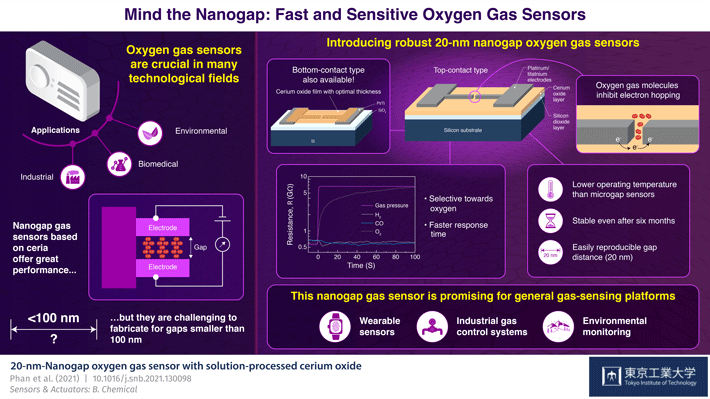
Nanogap gas sensors through a reliable and scalable fabrication strategy have been designed and produced by scientists at Tokyo Institute of Technology (Tokyo Tech). The gap between electrodes, which can be as small as 20 nm, allows for sensing oxygen with an unprecedented response time at relatively low temperatures, especially compared with microgap sensors. Their results pave the way towards general gas-sensing platforms for biomedical, industrial, and environmental applications.

Oxygen (O2) is an essential gas not only for us and most other lifeforms, but also for many industrial processes, biomedicine, and environmental monitoring applications. Given the importance of O2 and other gases, many researchers have focused on developing and improving gas-sensing technologies. At the frontier of this evolving field lie modern nanogap gas sensors—devices usually comprised of a sensing material and two conducting electrodes that are separated by a minuscule gap in the order of nanometers (nm), or thousand millionths of a meter. When molecules of specific gases get inside this gap, they electronically interact with the sensing layer and the electrodes, altering measurable electric properties such as the resistance between the electrodes. In turn, this allows one to indirectly measure the concentration of a given gas.
Although nanogap gas sensors bear many more attractive properties than the closely related microgap gas sensors, they have proven much more difficult to mass produce reliably for gap distances in the order of tens of nanometers. At the Laboratory for Materials and Structures of Tokyo Tech, a team of scientists led by Prof. Yutaka Majima is seeking ways to fabricate better nanogap sensors. In their latest study, which was published in Sensors & Actuators B: Chemical![]() , the team presents a new strategy to produce nanogap oxygen gas sensors using platinum/titanium (Pt/Ti) electrodes and a cerium oxide (CeO2) sensing layer.
, the team presents a new strategy to produce nanogap oxygen gas sensors using platinum/titanium (Pt/Ti) electrodes and a cerium oxide (CeO2) sensing layer.
Two sensor designs were tested by Prof. Majima and his team. In the bottom-contact design, the CeO2 sensing layer is first deposited onto a silicon substrate and the two Pt/Ti electrodes are laid on top of the CeO2 through electron beam lithography (EBL). With EBL, one draws custom shapes on a resist film using a focused beam of electrons with extreme precision. This then allows for the selective etching or evaporation of Pt/Ti regions, thus giving shape to the nanogap electrodes. The other design (top-contact) was produced using EBL as well, but the CeO2 was applied on top of the Pt/Ti electrodes as a thin coating layer.
With this fabrication strategy, the team managed to reliably produce stable Pt nanogaps as small as 20 nm, which was unprecedented in the literature. Both sensor designs exhibited similar and highly promising performances, as Prof. Majima remarks: "For a gap separation of 35 nm, our nanogap O2 gas sensors exhibited a fast response time of 10 seconds at a relatively low operating temperature of 573 K (300 °C); this response time is approximately three orders of magnitude shorter than that of microgap sensors under the same measurement conditions." Moreover, their procedure offers better scalability than those for previously developed nanogap gas sensors.
In addition to the sensor designs, this study provided important insights on the electron hopping mechanisms by which O2 molecules modulate the resistance between the Pt electrodes in the presence of CeO2 at the nanogap. Taken together, the results of this study are paving the way to better gas-sensing devices, as Prof. Majima concludes: "Our nanogap gas sensors could be promising candidates for the development of a general gas-sensing platform with a low operating temperature." In due time, nanogap gas sensors shall surely find their way into more fields of application, including wearable biomedical devices, industrial condition monitoring, and environmental sensing.
- Reference
| Authors : | Trong Tue Phan, Tsubasa Tosa, Yutaka Majima* |
|---|---|
| Title of original paper : | 20-nm-Nanogap oxygen gas sensor with solution-processed cerium oxide |
| Journal : | Sensors & Actuators B: Chemical |
| DOI : | 10.1016/j.snb.2021.130098 |
| Affiliations : |
Laboratory for Materials and Structures, Institute of Innovative Research, Tokyo Institute of Technology |
* Corresponding author's email: majima@msl.titech.ac.jp
- Elucidation of structural property in Li-ion batteries that deliver ultra-fast charging | Tokyo Tech News
- Beyond the limits of conventional electronics: stable organic molecular nanowires | Tokyo Tech News
- New aspect of atom mimicry for nanotechnology applications | Tokyo Tech News
- Majima Laboratory
- Researcher Profile | Tokyo Tech STAR Search - Yutaka Majima
- Laboratory for Materials and Structures
- Institute of Innovative Research (IIR)
- Materials Science and Engineering Graduate Major|Education|Department of Materials Science and Engineering, School of Materials and Chemical Technology
- Latest Research News
Further Information
Professor Yutaka Majima
Institute of Innovative Research,
Tokyo Institute of Technology
Email majima@msl.titech.ac.jp


