Materials Science and Engineering News
Giant Electronic Conductivity Change Driven by Artificial Switch of Crystal Dimensionality
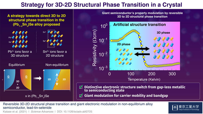
Scientists at Tokyo Institute of Technology demonstrate the artificial control of crystal structure dimensionality to switch electronic conductivity in three orders of magnitude. The scientist succeeded to induce the direct phase transition between three dimensional and two dimensional crystal structures in a lead-tin-selenide alloy semiconductor, which shows the abrupt band structure switch from a gap-less metallic state to a semiconducting state. The present result would lead to further functional property switching in semiconductors.
The electronic properties of solid materials are highly dependent on crystal structures and their dimensionalities (i.e., whether the crystals have predominantly 2D or 3D structures). As Professor Takayoshi Katase of Tokyo Institute of Technology notes, this fact has an important corollary: "If the crystal structure dimensionality can be switched reversibly in the same material, a drastic property change may be controllable." This insight led Prof. Katase and his research team at Tokyo Institute of Technology, in partnership with collaborators at Osaka University and National Institute for Materials Science, to embark on research into the possibility of switching the crystal structure dimensionality of a lead-tin-selenide alloy semiconductor. Their results appear in a paper published in a recent issue of the peer-reviewed journal Science Advances.
The lead-tin-selenide alloy, (Pb1-xSnx)Se is an appropriate focus for such research because the lead ions (Pb2+) and tin ions (Sn2+) favor distinct crystal dimensionalities. Specifically, pure lead selenide (PbSe) has a 3D crystal structure, whereas pure tin selenide (SnSe) has a 2D crystal structure. SnSe has bandgap of 1.1 eV, similar to the conventional semiconductor Si. Meanwhile, PbSe has narrow bandgap of 0.3 eV and shows 1 order of magnitude higher carrier mobility than SnSe. In particular, the 3D (Pb1-xSnx)Se has gathered much attention as a topological insulator. That is, the substitution for Pb with Sn in the 3D PbSe reduces the band gap and finally produces a gap-less Dirac-like state. Therefore, if these crystal structure dimensionality can be switched by external stresses such as temperature, it would lead to a giant functional phase transition, such as large electronic conductivity change and topological state transition, enhanced by the distinct electronic structure changes.
The alloying PbSe and SnSe would manipulate the drastic transition in structure, and such (Pb1-xSnx)Se alloy should induce strong frustration around phase boundaries. However, there is no direct phase boundary between the 3D PbSe and the 2D SnSe phases under thermal equilibrium. Through their experiments, Prof. Katase and his research team successfully developed a method for growing the nonequilibrium lead-tin-selenide alloy crystals with equal amounts of Pb2+ and Sn2+ ions (i.e., (Pb0.5Sn0.5)Se) that underwent direct structural phase transitions between 2D and 3D forms based on temperature. At lower temperatures, the 2D crystal structure predominated, whereas at higher temperatures, the 3D structure predominated. The low-temperature 2D crystal structure was more resistant to electrical current than the high-temperature 3D crystal was, and as the alloy was heated, its resistivity levels took a sharp dive around the temperatures at which the dimensionality phase transition occurred. The present strategy facilitates different structure dimensionality switching and further functional property switching in semiconductors using artificial phase boundary.
In sum, the research team developed a form of the semiconductor alloy (Pb1-xSnx)Se that undergoes temperature-dependent crystal dimensionality phase transitions, and these transitions have major implications for the alloy's electronic properties. When asked about the importance of his team's work, Prof. Katase notes that this form of the (Pb1-xSnx)Se alloy can "serve as a platform for fundamental scientific studies as well as the development of novel function in semiconductor technologies." This specialized alloy may, therefore, lead to exciting new semiconductor technologies with myriad benefits for humanity.
- Reference
| Authors : | Takayoshi Katase1,*, Yudai Takahashi1, Xinyi He1, Terumasa Tadano2, Keisuke Ide1, Hideto Yoshida3, Shiro Kawachi4, Junichi Yamaura4, Masato Sasase4, Hidenori Hiramatsu1,4, Hideo Hosono4, and Toshio Kamiya1,4,* |
|---|---|
| Title of original paper : | Reversible 3D-2D structural phase transition and giant electronic modulation in nonequilibrium alloy semiconductor, lead-tin-selenide |
| Journal : | Science Advances |
| DOI : | 10.1126/sciadv.abf2725 |
| Affiliations : |
1 Laboratory for Materials and Structures, Institute of Innovative Research, Tokyo Institute of Technology 2 National Institute for Materials Science 3 The Institute of Scientific and Industrial Research, Osaka University 4 Materials Research Center for Element Strategy, Tokyo Institute of Technology |
* Corresponding authors' emails: katase@mces.titech.ac.jp, kamiya.t.aa@m.titech.ac.jp
- Multiple Semiconductor Type Switching To Boost Thermoelectric Conversion of Waste Heat | Tokyo Tech News
- Having it Both Ways: A Combined Strategy in Catalyst Design for Suzuki Cross-Couplings | Tokyo Tech News
- Shedding Light on the Development of Efficient Blue-Emitting Semiconductors | Tokyo Tech News
- Filling the Void in Ammonia Synthesis: The Role of Nitrogen Vacancies in Catalysts | Tokyo Tech News
- Breakthrough ammonia synthesis that does not need precious metals | Tokyo Tech News
- Running on Empty: New Affordable Catalyst Relies on Nitrogen Vacancies to Produce Ammonia | Tokyo Tech News
- An 'exceptionally stable' single-atom catalyst: Single platinum atoms stabilized in C12A7 crystals | Tokyo Tech News
- A nanoscale lattice of palladium and yttrium makes for a superlative carbon-linking catalyst | Tokyo Tech News
- Efficient bottom-up synthesis of new perovskite material for the production of ammonia | Tokyo Tech News
- New design strategy brightens up the future of perovskite-based light-emitting diodes | Tokyo Tech News
- Finding a needle in a haystack: Discovery of Ti2InB2 for synthesizing layered TiB | Tokyo Tech News
- Lighting it up: A new non-toxic, cheap, and stable blue photoluminescent material | Tokyo Tech News
- Hideo Hosono's story of IGZO TFT development features in Nature Electronics | Tokyo Tech News
- High Performance Nitride Semiconductor for Environmentally Friendly Photovoltaics | Tokyo Tech News
- Highly efficient ammonia synthesis catalyst developed | Tokyo Tech News
- Research group at Tokyo Tech develops new material for the electron injection layer and transport layer of organic EL displays | Tokyo Tech News
- 2019 Tokyo Tech Challenging Research Award | Tokyo Tech News
- Tokyo Tech Researchers awarded the Ceramics Grand Prize | Tokyo Tech News
- Kamiya-Katase Group
- Researcher Profile | Tokyo Tech STAR Search - Takayoshi Katase
- Researcher Profile | Tokyo Tech STAR Search - Toshio Kamiya
- Researcher Profile | Tokyo Tech STAR Search - Hideo Hosono
- Laboratory for Materials and Structures
- Institute of Innovative Research (IIR)
- Materials Research Center for Element Strategy (MCES)
- Materials Science and Engineering Graduate Major|Education|Department of Materials Science and Engineering, School of Materials and Chemical Technology
- Latest Research News
Further Information
Associate Professor Takayoshi Katase
Institute of Innovative Research, Tokyo Institute of Technology
Email katase@mces.titech.ac.jp
Featured News
![]()