Materials Science and Engineering News
Multiple Semiconductor Type Switching To Boost Thermoelectric Conversion of Waste Heat
Scientists at Tokyo Institute of Technology (Tokyo Tech) demonstrate double charge carrier type switching of tin monoselenide (SnSe) semiconductor by doping of antimony (Sb). The SnSe carrier type switches from p-type to n-type, and re-switches to p-type as doping increases, due to the switching of major Sb substitution site from Se to Sn, promising reliable charge polarity control, leading to realization of SnSe-based p/n homojunction thermoelectric device for converting waste heat into electricity and new insights on impurity doping of compound semiconductors.
In recent years, the energy consumption in developed countries has been rather wasteful. Nearly two-thirds of the total energy is typically discarded into the environment as "waste heat," which ends up contributing to global warming. Finding a way to productively use this heat has been at the forefront of every material researcher's priority.
One of the various possible ways to recover this waste heat as electricity is using what is known as "thermoelectric conversion"—a process that uses temperature difference in semiconductors to directly convert into electric voltage. Thermoelectric devices include p-type and n-type semiconductors with two types of charge carriers, i.e. electron and hole. The p-type and n-type semiconductors are connected in series to produce a large thermoelectric voltage (Figure 1). Therefore, it is necessary to develop the both p-type and n-type semiconductors with high thermoelectric conversion efficiency.
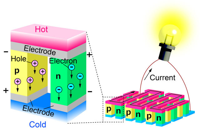
Figure 1. Thermoelectric device that converts waste heat into electricity
- Tin monoselenide (SnSe), when doped with antimony (Sb), can make for a suitable candidate for the design of thermoelectric conversion elements (p-n junction device).
One particular semiconductor material that scientists have recently turned their attention to is tin monoselenide (SnSe), which reportedly exhibits the world's highest thermoelectric conversion performance index ZT value. However, SnSe is incapable of controlling the charge carrier type with ease. Doping with alkali ions improves p-type thermoelectric performance but the alkali ions are volatile and diffusive elements, and are not suitable for high-temperature applications. Adding bismuth and iodine to make it n-type, on the other hand, results in low electron concentrations.
In a new study published in Advanced Functional Materials, a team of scientists from Tokyo Tech, Japan, led by Prof. Takayoshi Katase discovered that when doped with antimony (Sb), SnSe, denoted as (Sn1-xSbx)Se, exhibits a peculiar switching of conduction type. Specifically, the team observed that at low doping concentrations, (Sn1-xSbx)Se started out with p-type conduction but switched to n-type with increasing doping, and finally switched back to p-type for high concentrations (see Figure 2). The elaborate analyses and calculations revealed an interesting charge type switching mechanism which, the team found, has to do with the distribution of Sb substitution sites between Sn and Se. They attributed this switching behavior to a switching of major Sb substitution site from Se (SbSe) to Sn (SbSn) with increasing doping.
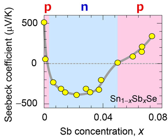
Figure 2. Change in thermoelectromotive force (Seebeck coefficient) with addition of Sb impurity to SnSe
- SnSe starts out with p-type conduction at low Sb concentrations (<0.5%), changes to n-type at intermediate concentrations (0.5%<x<5%), and switches back to p-type at high concentrations (x>0.5%).
Scientists explained that at very low Sb concentrations, the p-type conduction occurs solely due to holes supplied by Sn vacancy. But as doping increases, SbSn starts to donate electrons while SbSe forms an "impurity band" that allows conduction through it, resulting in the observed n-type behavior. However, as doping level goes up further, the Fermi level approaches the midgap level located between the SbSe impurity band and conduction band minimum, resulting in the p-type conduction.
With such remarkable insights to offer, the results are undoubtedly a potential game changer for SnSe. However, Prof. Takase foresees an even broader scope. "Now that we understand the mechanism at play in the polarity switching of Sb-doped SnSe, we can hope to optimize the bulk synthesis process to further improve its thermoelectric performance and, in turn, realize high-performance thermoelectric conversion devices with it," surmises Prof. Katase.
What's more, the researchers also expect that the doping-site-switching based polarity control will become more versatile in the future and can be applied to other semiconductor materials whose carrier types are difficult to control otherwise. Here's hoping that this leads to a future where waste heat won't be a waste anymore!
- Reference
| Authors : | Chihiro Yamamoto1, Xinyi He1, Takayoshi Katase1,*, Keisuke Ide1, Yosuke Goto2, Yoshikazu Mizuguchi2, Akane Samizo3, Makoto Minohara4, Shigenori Ueda5, Hidenori Hiramatsu1,6, Hideo Hosono6 and Toshio Kamiya1,6,* |
|---|---|
| Title of original paper : | Double charge polarity switching in Sb-doped SnSe with switchable substitution sites |
| Journal : | Advanced Functional Materials |
| DOI : | 10.1002/adfm.202008092 |
| Affiliations : | 1 Laboratory for Materials and Structures, Institute of Innovative Research, Tokyo Institute of Technology 2 Department of Physics, Tokyo Metropolitan University 3 Department of Materials Science and Technology, Tokyo University of Science 4 Research Institute for Electronics and Photonics, National Institute of Advanced Industrial Science and Technology 5 Research Center for Advanced Measurement and Characterization, National Institute for Materials Science 6 Materials Research Center for Element Strategy, Tokyo Institute of Technology |
* Corresponding authors' emails: katase@mces.titech.ac.jp, kamiya.t.aa@m.titech.ac.jp
- Having it Both Ways: A Combined Strategy in Catalyst Design for Suzuki Cross-Couplings | Tokyo Tech News
- Shedding Light on the Development of Efficient Blue-Emitting Semiconductors | Tokyo Tech News
- Filling the Void in Ammonia Synthesis: The Role of Nitrogen Vacancies in Catalysts | Tokyo Tech News
- Breakthrough ammonia synthesis that does not need precious metals | Tokyo Tech News
- Running on Empty: New Affordable Catalyst Relies on Nitrogen Vacancies to Produce Ammonia | Tokyo Tech News
- An 'exceptionally stable' single-atom catalyst: Single platinum atoms stabilized in C12A7 crystals | Tokyo Tech News
- A nanoscale lattice of palladium and yttrium makes for a superlative carbon-linking catalyst | Tokyo Tech News
- Efficient bottom-up synthesis of new perovskite material for the production of ammonia | Tokyo Tech News
- New design strategy brightens up the future of perovskite-based light-emitting diodes | Tokyo Tech News
- Finding a needle in a haystack: Discovery of Ti2InB2 for synthesizing layered TiB | Tokyo Tech News
- Lighting it up: A new non-toxic, cheap, and stable blue photoluminescent material | Tokyo Tech News
- Hideo Hosono's story of IGZO TFT development features in Nature Electronics | Tokyo Tech News
- High Performance Nitride Semiconductor for Environmentally Friendly Photovoltaics | Tokyo Tech News
- Highly efficient ammonia synthesis catalyst developed | Tokyo Tech News
- Research group at Tokyo Tech develops new material for the electron injection layer and transport layer of organic EL displays | Tokyo Tech News
- 2019 Tokyo Tech Challenging Research Award | Tokyo Tech News
- Tokyo Tech Researchers awarded the Ceramics Grand Prize | Tokyo Tech News
- Kamiya-Katase Group
- Researcher Profile | Tokyo Tech STAR Search - Takayoshi Katase
- Researcher Profile | Tokyo Tech STAR Search - Toshio Kamiya
- Researcher Profile | Tokyo Tech STAR Search - Hideo Hosono
- Laboratory for Materials and Structures
- Institute of Innovative Research (IIR)
- Materials Research Center for Element Strategy (MCES)
- Materials Science and Engineering Graduate Major|Education|Department of Materials Science and Engineering, School of Materials and Chemical Technology
- Latest Research News
Further Information
Associate Professor Takayoshi Katase
Institute of Innovative Research,
Tokyo Institute of Technology
Email: katase@mces.titech.ac.jp
Featured News
![]()