Materials Science and Engineering News
A low-voltage high-luminance perovskite LED realized — press event held
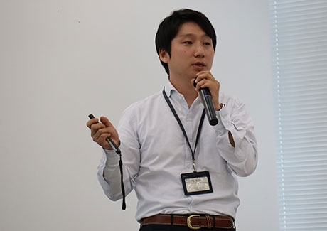
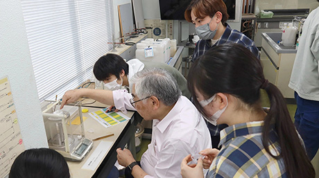
On July 17 at Ookayama Campus, Honorary Professor Hideo Hosono and Assistant Professor Junghwan Kim of the Materials Research Center for Element Strategy held a press event showcasing their new low-voltage, high-luminance perovskite LED.
The Materials Research Center for Element Strategy develops breakthrough materials to address issues arising from dependence on rare elements. At the press event, the researchers explained how using a new transparent semiconductor (amorphous Zn-Si-O, abbreviated a-ZSO), composed of earth abundant elements, that has a low work function1 yet high electron mobility for the electron transport layers allowed for the realization of a low-voltage, high-luminance perovskite2 LED.
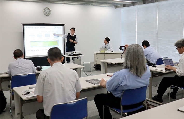
The press event
Key points in the development
Organic electroluminescence (EL) is commonly used in the displays of televisions, smartphones, and other devices. The appeal of organic EL is in the self-light emiting and its ability to provide quality images. However, shortcomings also exist in the form of short lifetime and high operating voltage requirements. Therefore, new luminescent materials are being sought to solve these problems.
Device displays need to meet various performance requirements, including high resolution and accurate color reproduction. Perovskite LEDs are gaining attention for their capacity to reproduce colors. They have high chromatic purity and the additional advantage of being manufacturable using solution processing.
While numerous researchers are studying low-dimensional perovskite, Hosono and Kim demonstrated successfully that three-dimensional perovskite crystals would be better suited to LEDs, in which electric current, not light, is introduced, because they transport electrons and electron holes more easily. The researchers created a perovskite LED by placing perovskite crystal adjacent to a layer of a-ZSO, a semiconductor suitable for introducing electrons from an electrode to the luminescent layer. The green LED achieved a brightness of 10,000 cd/m2 at 2.9 V and 500,000 cd/m2 at 5 V. The maximum brightness of an average smartphone is about 400 cd/m2, making the new LED extremely bright.
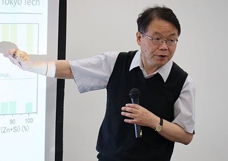
of the Materials Research Center for Element Strategy
What next?
High brightness has been achieved for green and red LEDs, but there is still room for improvement for blue LEDs. The concepts developed in the study have proved to be highly effective, and taking them further for new materials may lead to the next-generation in LEDs.
The minimum energy required to remove an electron from a material. Thermionic emission from metal surfaces and electron emission due to electric fields occur less in metals with a higher work function.
A type of crystalline structure. Huge variety of atoms may be incorporated to together to form its structure. Application in LEDs is being considered due to its light absorption, charge transportability, and other properties.
- New design strategy brightens up the future of perovskite-based light-emitting diodes | Tokyo Tech News
- Hosono-Kamiya Laboratory
- Researcher Profile | Tokyo Tech STAR Search - Hideo Hosono
- Researcher Profile | Tokyo Tech STAR Search - Junghwan Kim
- Materials Research Center for Element Strategy
- Latest Research News
Contact
Public Relations Section, Tokyo Institute of Technology
Email media@jim.titech.ac.jp
Tel +81-3-5734-2975
Featured News
![]()